


– 9 –
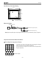
ICX274AQ
VHL
VCR
twl
two
twh
Vφ
H
VφH
2
tr
Hφ
2β
90%
10%
Hφ
1β
tf
RG waveform
V
RGLH
V
RGH
V
RGL
V
RGLL
V
RGLm
tr twh
twl
tf
Vφ
RG
Point A
V
SUB
(Internally generated bias)
100%
90%
10%
0%
tr tftwh
φM
2
φM
Vφ
SUB
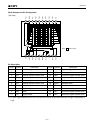
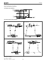
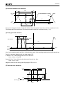
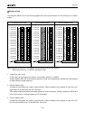
(3) Horizontal transfer clock waveform
Cross-point voltage for the Hφ1β rising side of the horizontal transfer clocks Hφ1β and Hφ2β waveforms is VCR.
The overlap period for twh and twl of horizontal transfer clocks Hφ1β and Hφ2β is two. (β = A, B)
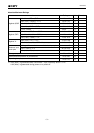
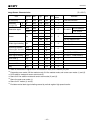
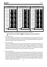
(4) Reset gate clock waveform
VRGLH is the maximum value and VRGLL is the minimum value of the coupling waveform during the period from
Point A in the above diagram until the rising edge of RG.
In addition, VRGL is the average value of VRGLH and VRGLL.
VRGL = (VRGLH + VRGLL)/2
Assuming VRGH is the minimum value during the interval twh, then:
VφRG = VRGH – VRGL
Negative overshoot level during the falling edge of RG is VRGLm.
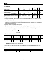
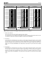
(5) Substrate clock waveform