


T
T
T
S
S
S
8
8
8
G
G
G
~
~
~
1
1
1
6
6
6
G
G
G
C
C
C
F
F
F
6
6
6
0
0
0
0
0
0
600X CompactFlash Card
Transcend Information Inc.
V1.0
18
state and 100 A high state, including pull-up resistor. The card shall be able to drive at least the following load
10
while meeting all AC timing requirements: 50 pF at a DC current of 400 A low state and 100 A high state.
4) Status Signals: the socket shall present a load to the card no larger than 50 pF
10
at a DC current of 400 A low
state and 100 A high state, including pull-up resistor. The card shall be able to drive at least the following load
10
while meeting all AC timing requirements: 50 pF at a DC current of 400 A low state and 100 A high state.
5) Status Signals: the socket shall present a load to the card no larger than 50 pF
10
at a DC current of 400 A low
state and 100 A high state, including pull-up resistor. The card shall be able to drive at least the following load
10
while meeting all AC timing requirements: 50 pF at a DC current of 400 A low state and 1100 A high state.
6) BVD2 was not defined in the JEIDA 3.0 release. Systems fully supporting JEIDA release 3 SRAM cards shall
pull-up pin 45 (BVD2) to avoid sensing their batteries as “Low.”
7) Address Signals: each card shall present a load of no more than 100pF
10
at a DC current of 450 A low state and
150 A high state. The host shall be able to drive at least the following load
10
while meeting all AC timing
requirements: (the number of sockets wired in parallel) multiplied by (100pF with DC current 450 A low state
and 150 A high state per socket).
8) Data Signals: the host and each card shall present a load no larger than 50pF
10
at a DC current of 450 A and
150 A high state. The host and each card shall be able to drive at least the following load
10
while meeting all
AC timing requirements: 100pF with DC current 1.6mA low state and 300 A high state. This permits the host to
wire two sockets in parallel without derating the card access speeds.
9) Reset Signal: This signal is pulled up to prevent the input from floating when a CFA to PCMCIA adapter is used
in a PCMCIA revision 1 host. However, to minimize DC current drain through the pull-up resistor in normal
operation the pull-up should be turned off once the Reset signal has been actively driven low by the host.
Consequently, the input is specified as an I2Z because the resistor is not necessarily detectable in the input
current leakage test.
10) Host and card restrictions for CF Advanced Timing Modes and Ultra DMA modes: Additional Requirements for
CF Advanced Timing Modes and Ultra DMA Electrical Requirements for additional required limitations on the
implementation of CF Advanced Timing modes and Ultra DMA modes respectively.
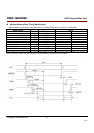
Additional Requirements for CF Advanced Timing Modes
The CF Advanced Timing modes include PC Card I/O and Memory modes that are 100ns or faster, PC Card Ultra
DMA modes 3 or above and True IDE PIO Modes 5,6, Multiword DMA Modes 3,4 and True IDE Ultra DMA modes
3 or above.
When operating in CF Advanced timing modes, the host shall conform to the following requirements:
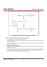
1) Only one CF device shall be attached to the CF Bus.
2) The host shall not present a load of more than 40pF to the device for all signals, including any cabling.
3) The maximum cable length is 0.15 m (6 in). The cable length is measured from the card connector to the host
controller. 0.46 m (18 in) cables are
not
supported.
4) The -WAIT and IORDY signals shall be ignored by the host.
Devices supporting CF Advanced timing modes shall also support slower timing modes, to ensure operability with
systems that do not support CF Advanced timing modes