


T
T
T
S
S
S
1
1
1
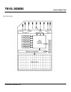
G
G
G
~
~
~
2
2
2
G
G
G
S
S
S
D
D
D
G
G
G
Secure Digital Card
Transcend Information Inc.
3
Bus Operating Conditions
• General
Parameter Symbol Min. Max. Unit Remark
Peak voltage on all lines -0.3 VDD+0.3 V
All Inputs
Input Leakage Current -10 10 µA
All Outputs
Output Leakage Current -10 10 µA
• Power Supply Voltage
Parameter Symbol Min. Max. Unit Remark
Supply voltage V
DD
2.0 3.6 V CMD0, 15,55,ACMD41
commands
Supply voltage specified in OCR register 2.7 3.6 V Except CMD0, 15,55,
ACMD41 commands
Supply voltage differentials (V
SS1
, V
SS2
) -0.3 0.3 V
Power up time 250 ms From 0v to V
DD
Min.
Note. The current consumption of any card during the power-up procedure must not exceed 10 mA.
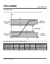
• Bus Signal Line Load
The total capacitance C
L
the CLK line of the SD Memory Card bus is the sum of the bus master capacitance C
HOST
, the bus
capacitance C
BUS
itself and the capacitance C
CARD
of each card connected to this line:
C
L
= C
HOST
+ C
BUS
+ Ν*C
CARD
Where N is the number of connected cards. Requiring the sum of the host and bus capacitances not to exceed 30 pF for
up to 10 cards, and 40 pF for up to 30 cards, the following values must not be exceeded:
Parameter Symbol Min. Max. Unit Remark
Bus signal line capacitance C
L
100 pF f
PP
≤ 20 MHz, 7 cards
Single card capacitance C
CARD
10 pF
Maximum signal line inductance 16 nH f
PP
≤ 20 MHz
Pull-up resistance inside card (pin1) R
DAT3
10 90 kΩ May be used for card
detection
Note that the total capacitance of CMD and DAT lines will be consist of C
HOST
, C
BUS
and one C
CARD
only since they are
connected separately to the SD Memory Card host.
Parameter Symbol Min. Max. Unit Remark
Pull-up resistance R
CMD
, R
DAT
10 100 kΩ To prevent bus floating
Bus signal line capacitance C
L
250 pF f
PP
≤ 5 MHz, 21 cards