EPSON Stylus COLOR 3000
Rev. A
2-1
2.3 Electrical Circuit Operation Principles
This printer consists of the following circuit board:
C203 MAIN board
C178 PSB/PSE board
C203 Panel board
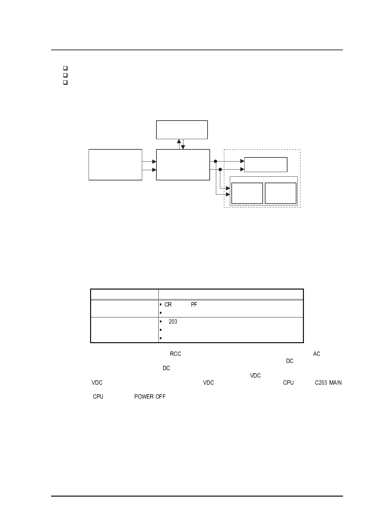
Head driver circuits are directly attached to the black and color printheads. Figure 2-13 shows the block
diagram of the electrical circuit.
2.3.1 C172 PSB/PSE Electrical Circuit Board
The output voltages of the PSB/PSE board are as shown in Table 2-7. Since the electrical circuit of this
printer is in a secondary circuit, the delay timer can be used to allows the printer to execute the capping
operation after the printer power is turned off. This is to prevent ink clogging or smudging caused by the
exposed condition of the printhead.
VDC Application
+42 V
motor/ motor
Printhead common voltage
+5 V
C MAIN control board (logic)
Sensors
Control panel, Head nozzle selection
The electrical circuit of this board uses the (Ringing Choke Converter) switching regulator. voltage
is first input to the filter circuit for higher harmonics absorption and is converted into voltage thorough
the rectifier and smoothing circuits. The voltage is then input to the switching circuit. These operations
are followed by the transformer which generates and stabilizes +42 in the secondary side. The
produced +42 is then converted into the stable +5 by the regulator IC. The on the
board monitors the on/off signal from the power switch on the control panel. When the power switch is
turned off, the sends the signal (PSC) to the electrical circuit. The electrical board has a
delay circuit (ZD86, C82 and Q84) to delay the power off. The delay period depends on the electrolytic
capacitor. It continues to output +5 V and +42 V to keep the main circuit switch on the primary side active
until all electric charge is discharged. The minimum delay period is normally 30 seconds, which ,however,
varies depending on the capacitor size.
+5VDC
+42VDC
C172 PSB/PSE
C203 PNL
C203 MAIN
Printer Mechanism Unit
CR/PF/Pump
Motors
CR Unit
Color Head
Driver Circuit
Black Head
Driver Circuit
Figure 2-13. Electrical Circuit Block Diagram
Table 2-7. DC Voltage Distribution


