


2-3
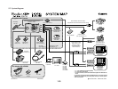
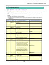
CHAPTER 2. TECHNICAL DESCRIPTION
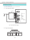
2.2 Signal Processing
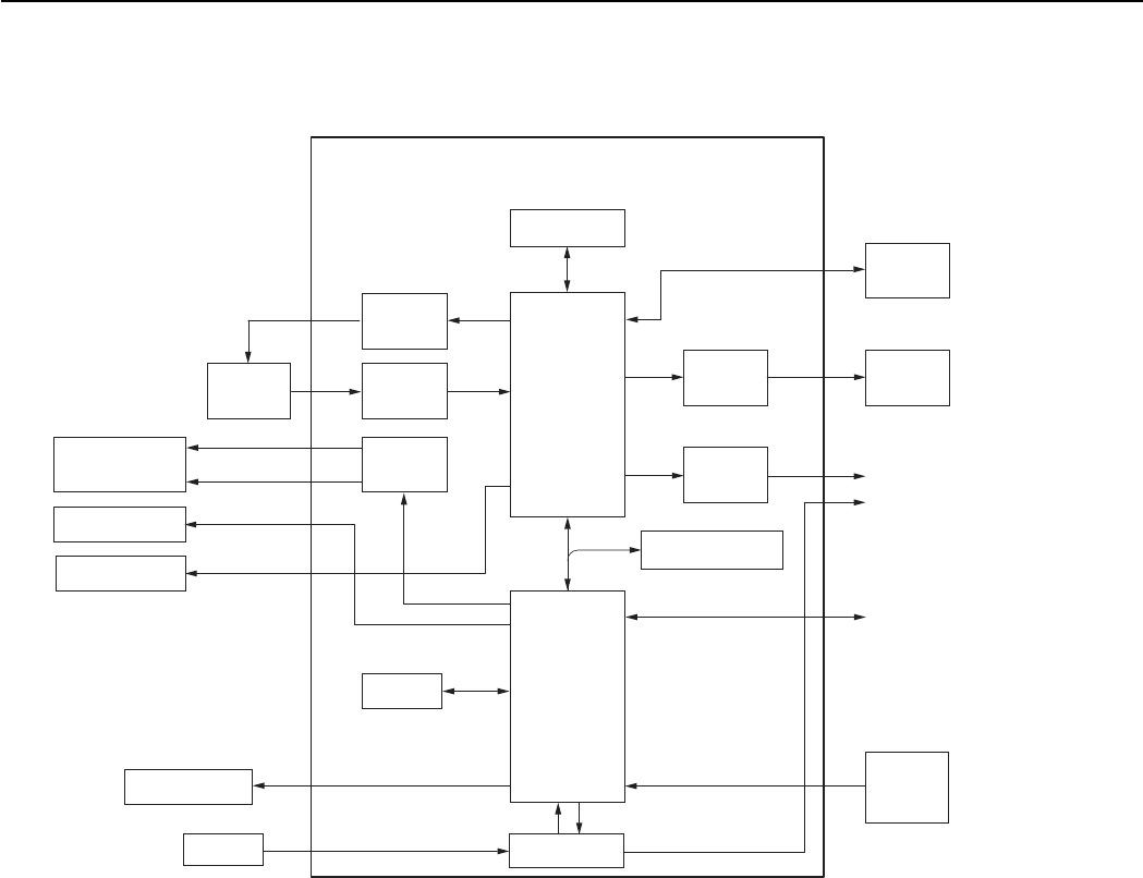
Fig. 3 Signal System Block Diagram
2.2.1 System Control
The CPU on the main PCB ass’y controls the EF lens (motor, shutter), operation switch receiver, USB
communication and flowing circuits.
• TG: Creation of the CCD drive pulse
• CDS, A/D: CCD signal processing and conversion of the digital data
• LCD Driver: Driving the LCD
• FLASH MEMORY: Firmware memory
• DSP: Picture processing
• RTC: Clock count for watch
• AF Support LED: AF auxiliary, self-timer and red-eye protection also serves as a lamp
• Electric Flash: Flash and charging circuit
CDS, A/D
LCD
Driver
CCD
Sensor
TG
Drive
Pulse
HD, VD
CLK
EF LENS
Motor
Driver
AF Support LED
FINDER LED
Electric FLASH
CF card
LCD
Video
Amp
RTC
MIC
FLASH MEMORY
AUDIO AMP
DSP
CPU
SW
DIAL
KEY
MAIN PCB ASS'Y
SDRAM
USB
VIDEO OUT
AUDIO OUT