


T
T
T
S
S
S
1
1
1
6
6
6
G
G
G
~
~
~
6
6
6
4
4
4
G
G
G
C
C
C
F
F
F
4
4
4
0
0
0
0
0
0
400X CompactFlash Card
Transcend Information Inc.
V1.0
36
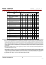
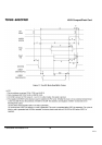
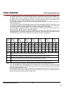
Notes: 1) The parameters tUI, tMLI : (Ultra DMA Data-In Burst Device Termination Timing and Ultra DMA Data-In
Burst Host Termination Timing), and tLI indicate sender-to-recipient or recipient-to-sender interlocks, i.e.,
one agent (either sender or recipient) is waiting for the other agent to respond with a signal before
proceeding. tUI is an unlimited interlock that has no maximum time value. tMLI is a limited time-out that
has a defined minimum. tLI is a limited time-out that has a defined maximum.
2) 80-conductor cabling shall be required in order to meet setup (tDS, tCS) and hold (tDH, tCH) times in
modes greater than 2.
3) Timing for tDVS, tDVH, tCVS and tCVH shall be met for lumped capacitive loads of 15 and 40 pF at the
connector where the Data and STROBE signals have the same capacitive load value. Due to reflections
on the cable, these timing measurements are not valid in a normally functioning system.
4)For all modes the parameter tZIORDY may be greater than tENV due to the fact that the host has a
pull-up on IORDY- giving it a known state when released.
5)The parameters tDS, and tDH for mode 5 are defined for a recipient at the end of the cable only in a
configuration with a single device located at the end of the cable. This could result in the minimum values
for tDS and tDH for mode 5 at the middle connector being 3.0 and 3.9 ns respectively.
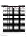
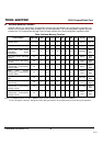
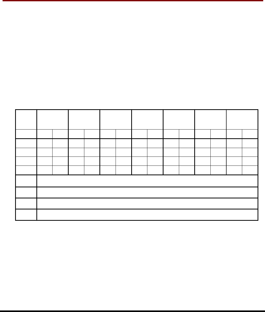
Name
UDMA
Mode 0
(ns)
UDMA
Mode 1
(ns)
UDMA
Mode 2
(ns)
UDMA
Mode 3
(ns)
UDMA
Mode4
(ns)
UDMA
Mode 5
(ns)
UDMA
Mode 6
(ns)
Min
Max
Min
Max
Min
Max
Min
Max
Min
Max
Min
Max
Min
Max
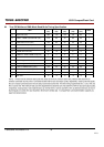
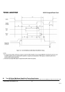
t
DSIC
14.7
9.7
6.8
6.8
4.8
2.3
2.3
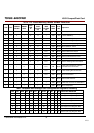
t
DHIC
4.8
4.8
4.8
4.8
4.8
2.8
2.8
t
DVSIC
72.9
50.9
33.9
22.6
9.5
6.0
5.2
t
DVHIC
9.0
9.0
9.0
9.0
9.0
6.0
5.2
t
DSIC
Recipient IC data setup time (from data valid until STROBE edge) (see note 2)
t
DHIC
Recipient IC data hold time (from STROBE edge until data may become invalid) (see note 2)
t
DVSIC
Sender IC data valid setup time (from data valid until STROBE edge) (see note 3)
t
DVHIC
Sender IC data valid hold time (from STROBE edge until data may become invalid) (see note 3)
Notes: 1) All timing measurement switching points(low to high and high to low) shall be taken at 1.5 V.
2) The correct data value shall be captured by the recipient given input data with a slew rate of 0.4 V/ns
rising and falling and the input STROBE with a slew rate of 0.4 V/ns rising and falling at tDSIC and tDHIC
timing (as measured through 1.5 V).
3)The parameters tDVSIC and tDVHIC shall be met for lumped capacitive loads of 15 and 40 pF at the IC
where all signals have the same capacitive load value. Noise that may couple onto the output signals from
external sources has not been included in these values.