


26
Appendix
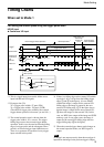
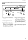
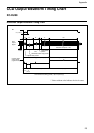
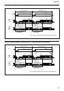
Vertical Output Waveform Timing Chart (2:1 interlaced frame accumulation)
* The transfer stop period is included in the dummy bits.
305 H 305 H
13579
579
581
2468
580
7.5 H
7.5 H
VD
287.5
6141 3.5
287.5
61423
582
Odd field (312.5 H) Even field (312.5 H)
CCD
output
signal
Camera
video
output
signal
Optical black portion
Empty
transfer
Optical black portion
Empty
transfer
Vertical blanking
period (25 H)
Vertical blanking
period (25 H)
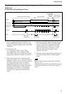
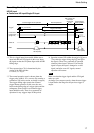
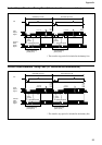
Vertical Output Waveform Timing Chart (2:1 interlaced field accumulation)
* The transfer stop period is included in the dummy bits.
305 H 305 H
1
2+3
4+5
6+7
8+9
582
1+2
3+4
5+6
7+8
578+579
580+581
579+580
7.5 H 7.5 H
VD
287.5287.5
6141 3.5 614
1
3
581+582
Odd field (312.5 H) Even field (312.5 H)
CCD
output
signal
Camera
video
output
signal
Optical black portion
Empty
transfer
Optical black portion
Empty
transfer
Vertical blanking
period (25 H)
Vertical blanking
period (25 H)