


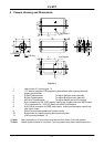
CV-M77
5.4 Input and Output Circuits
In the following schematic diagrams the input and output circuits for video and timing signals are
shown. For alternative connections refer to “Internal Switch and Jumper Settings”. Jumper
settings are shown as for factory default.
5.4.1 Video input
The video output signal is a 75Ω RGB video
signal. The signal level is 0.7Vpp.
Composite sync. is selectable on the green
video signal via software or the internal switch
302-3. The sync. signal level is 0.3Vpp.
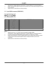
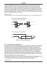
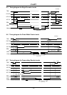
5.4.2 Trigger input
The trigger input is AC coupled with a flip-flop.
The input signal level is 4V ± 2V.
The trigger input impedance is 1.2 kΩ or 75Ω
selectable via the internal switch S301-3.
SC104V
SC102V
SC102V
33KB
100KB
33KB
1K8B
75C
S301-3
GND
Trigger
input
+5V
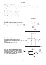
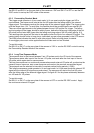
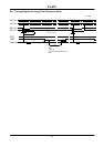
5.4.3 HD and VD input
The HD and VD input circuit can be 75Ω
terminated via the internal switch S301-1 and
S301-2.
The input signal level is 4V ± 2V.
SC104V
SC102V
33KB
1K8B
75C
S301-1(HD),2(VD)
GND
HD, VD
input
+5V
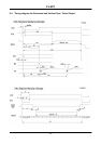
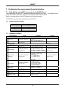
5.4.4 HD, VD, PCLK, WEN and EEN output
The output circuits for these signals are 75Ω
complementary emitter followers. The single
circuit delivers a TTL signal. The output level
≥ 4 V from 75Ω (no termination).
Int VD
Int HD
PCKL
WEN
EEN
10KB
120C
150C
10KB
220B
TTL
+5V
- 9 -