CV-A11
5.3. Input and Output Circuits
In the following schematic diagrams the input and output circuits for video and timing signals
are shown. For alternative connections refer to “10.1. CV-A11 emulating CV-M10 interfacing.”
Jumper settings are shown as for factory default.
5.3.1. Video output
GND
#4/12
75
Video
Output
NC
82p
2µ7
CXA1310
32
300 mV
420 mV
L
BNC
GND
#4/12
75
Video
Output
NC
82p
2µ7
CXA1310
32
300 mV
420 mV
L
BNC
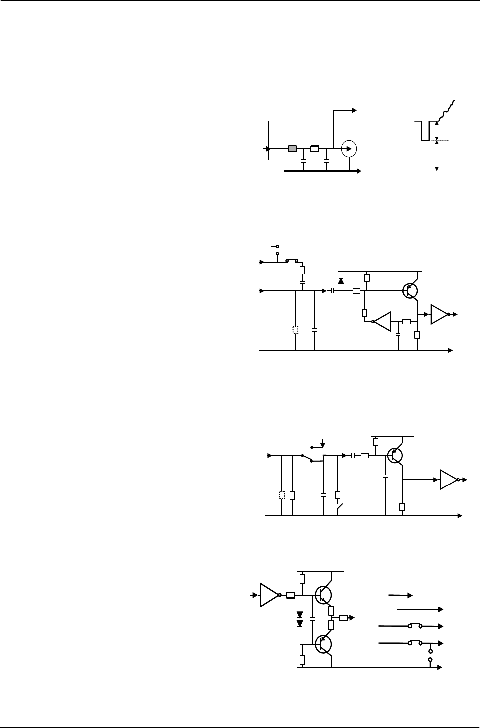
The video output is a 75 Ω DC coupled
circuit. The BNC connector and pin #4 on
the 12-pin connector is in parallel. Avoid
double termination. The video DC level is
shown with 75 Ω termination.
Fig. 4. Video output.
5.3.2. Trigger input
The trigger input is AC coupled. To allow a
long pulse width, the input circuit is a flip
flop, which is toggled by the negative or
positive differentiated spikes caused by
the falling or rising trigger edges.
GND
+5V
33k
TTL
1k
GND
100n
1k
Trigger
input
33k
100k
1n
NCNC
#5/6
JP4#11/12
100
100n
+12v
JP1
GND
+5V
33k
TTL
1k
GND
100n
1k
Trigger
input
33k
100k
1n
NCNC
#5/6
JP4#11/12
100
100n
+12v
JP1
The trigger polarity can be changed.
Trigger input level 4 V ±2 V.
The trigger-input impedance is 1 kΩ.
JP1 and JP4 are for alternative
configuration for pin #10.
Fig. 5. Trigger input.
5.3.3. HD and VD input
+5V
47p
33k
TTL
1k2
GND
10µ
4k7
VD HD
Input/output
+
75
SW2
1k
1n
NC
From VD HD
output
SW1
+5V
47p
33k
TTL
1k2
GND
10µ
4k7
VD HD
Input/output
+
75
SW2
1k
1n
NC
From VD HD
output
SW1
The input circuit for external HD and VD
signals are shown. It can be 75 Ω terminated
by closing SW2. SW1 will switch to output the
internal HD and VD signal.
HD and VD input level is 4 V ±2 V.
Fig. 6. HD and VD input.
5.3.4. HD, VD, PCLK, WEN and EEN output
Output circuit for these signals are 75 Ω
complementary emitter followers. It will
deliver a full TTL signal. JP5 and JP3 are for
alternative configuration for pin #10.
GND
+5V
10
10
10k
10k
67
TTL
220
VD, HD
WEN/ EEN
PCLK
WEN
#10/12
#6/6
#9/12
SW1
JP3
JP2
JP5
GND
+5V
10
10
10k
10k
67
TTL
220
VD, HD
WEN/ EEN
PCLK
WEN
#10/12
#6/6
#9/12
SW1
JP3
JP2
JP5
Output level ≥4 V from 75Ω. (No
termination).
The WEN polarity can be changed.
Signal on pin #6/6 can be changed.
Fig. 7. HD, VD, PCLK, WEN and EEN output.
- 5 -


