


– 3 –
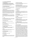
1A
1
1Y
2
2A
3
2Y
4
3A
5
3Y
6
GND
7
4Y
8
4A
9
5Y
10
5A
11
6Y
12
6A
13
V
CC
14
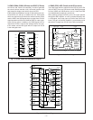
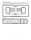
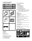
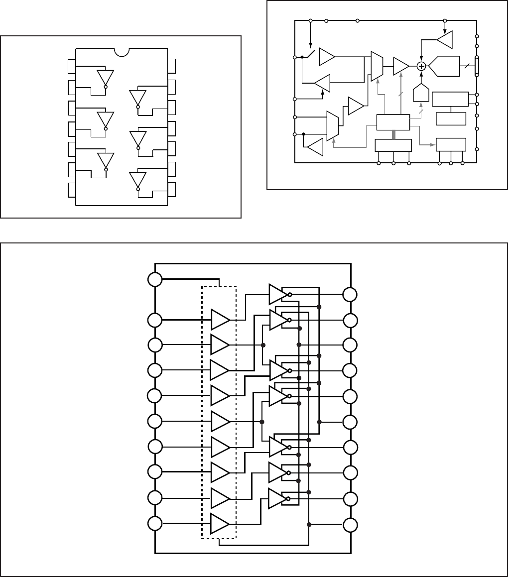
Fig. 1-3. IC902, IC904 and IC908 Block Diagram
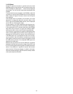
Fig. 1-4. IC907 Block Diagram
3. IC902, IC904, IC908 (H Driver) and IC907 (V Driver)
An H driver and V driver are necessary in order to generate
the clocks (vertical transfer clock, horizontal transfer clock
and electronic shutter clock) which driver the CCD.
IC902, IC904 and IC908 are inverter IC which drives the hori-
zontal CCDs (H1 and H2). In addition the XV1-XV3 signals
which are output from IC102 are the vertical transfer clocks,
and the XSG1 and XSG signal which is output from IC102 is
superimposed onto XV2A and XV2B at IC907 in order to gen-
erate a ternary pulse. In addition, the XSUB signal which is
output from IC102 is used as the sweep pulse for the elec-
tronic shutter, and the RG signal which is output from IC102
is the reset gate clock.
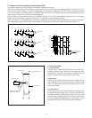
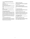
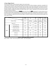
4. IC905 (CDS, AGC Circuit and A/D Converter)
The video signal which is output from the CCD is input to Pin
(30) of IC905. There are S/H blocks inside IC905 generated
from the XSHP and XSHD pulses, and it is here that CDS
(correlated double sampling) is carried out.
After passing through the CDS circuit, the signal passes
through the AGC amplifier. It is A/C converted internally into
a 10-bit signal, and is then input to IC102 of the CA2 circuit
board. The gain of the AGC amplifier is controlled by serial
data which is output from IC102 of the CA2 circuit board.
Fig. 1-5. IC905 Block Diagram
SHT
V3B
V
L
V3A
V
H
V1B
V1A
GND
V4
V2
XV2
V
DD
XSHT
XSG3B
XSG3A
XV1
XSG1B
XSG1A
XV4
Input
Buffer
XV3
CCDIN
CLPDM
AUX1IN
AUX2IN
SDATA
SCK
SL
SEN
DATA
CLK
SHDSHP
DVSS
DVDD
VRT
VRB
DRVDD
DRVSS
DOUT
CLPOB
AVSS
AVDD
PBLK
CLP
2:1
MUX
BUF
CLP
CONTROL
REGISTERS
DIGITAL
INTERFACE
CDS
2:1
MUX
10
8
VGA
INTERNAL
TIMING
INTERNAL
BIAS
BANDGAP
REFERENCE
10-BIT
ADC
CLP
4 dB
Offset
DAC
AD9840
10
2~36 dB
CML