


CHAPTER 4 IMAGE FORMATION SYSTEM
COPYRIGHT
©
1999 CANON INC. CANON PC800s/900s REV.0 AUG. 1999 PRINTED IN JAPAN (IMPRIME AU JAPON)
4-10
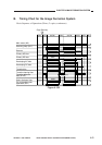
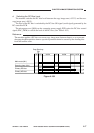
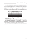
STBY INTR SCFW SCFWSCRV LSTR
STBY
Main motor (M1)
Reference bias (ATVC)
Transfer bias
SCRV
0.7sec (approx.)
0.8sec (approx.)
Copy Start key
ON
1.2sec (approx.)
Cleaning bias
1.6sec(approx.)
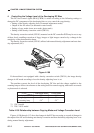
Figure 4-106
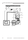
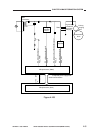
c. Correcting the Transfer Bias Voltage Level (ATVC control)
The machine automatically corrects the application voltage level of the transfer bias to correct
the changes in the transfer efficiency caused by the deterioration of the transfer roller or the
changes in the environment.
A current of a specific level (-14.6 µA) is applied to the transfer charging roller during initial
rotation executed each time the Copy Start key is pressed. The microprocessor (Q900) on the com-
posite power supply PCB checks the transfer current detection signal (T_FW_S), and varies the
transfer bias applied to the transfer charging roller so that it will be an appropriate level.
Reference:
While the transfer charging roller makes a single rotation, the microprocessor (Q900) checks
the transfer current detection signal four times, and determines the level of the transfer bias to
apply using the average of the readings.
d. Switching the Polarity of the Transfer Bias (cleaning bias)
The machine uses a direct charging method, allowing toner to move from the photosensitive
drum to the transfer roller as when a jam occurs if left unattended.
To remove excess toner, a positive voltage is applied to the transfer roller as follows, thereby
returning the toner from the roller to the drum:
< Timing >
• While initial rotation is executed after the Copy Start key is pressed
• Part of the period in which the scanner is moved in reverse
• Part of the period in which last rotation is executed
The polarity of the transfer bias is switched by the transfer bias ON signal (serial signal) gener-
ated by the DC controller PCB.
In response to the signal, the microprocessor (Q900) on the composite power supply PCB
causes the transfer positive DC bias On signal (T_REV_ON*) to go ‘0’, so that the positive compo-
nent of the transfer bias (constant current control, + 1.56µA/2.5 kV max.) will be applied to the
transfer roller. (See Table 4-103.)