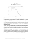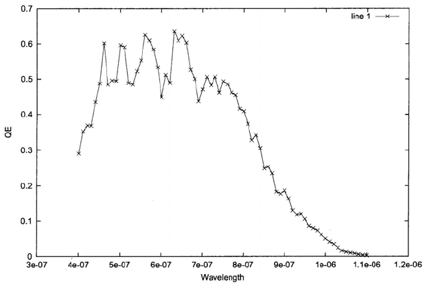
Figure 1.3.1
RDI and MRDI Responsivity Curve
1.4 Image Sensor
Pixel level processing image sensors are based on the principle that photons induced by charge at
the pixel site should be converted to, as nearly as possible, a noise-free signal at the pixel site.
The application of this principle produces the lowest possible noise and also allows signal control
at each pixel.
As is true in other sensors, photons induce charge which is collected on a capacitor at the photo
site. In a pixel level processing sensor, this charge is converted to an amplified voltage at the
pixel. This voltage is then read out through a multiplexor to an external circuit. Since the readout
starts with a strong signal, the dominant read noise source is the noise associated with the charge
accumulation at the pixel.
The 2048 x 1 linear CMOS image sensor uses a low fixed pattern noise capacitive transimpedance
amplifier (LFPN CTIA) pixel architecture. The pixel also includes circuitry for reducing 1/f noise,
correlated double sampling, electronic shuttering, and a horizontal anti-blooming drain. High speed
non-destructive readout of the sensor is achieved by using a hierarchial readout structure with two
output ports.
In simplified form, the pixel integration cycle consists of three steps: 1) reset the capacitor to fully
charged, 2) accumulate electrons on the capacitor, and 3) read the resulting charge value.
Conventionally these steps have been done by sensor-wide controls. Use of pixel level processing
results in at least an order of magnitude reduction in noise due to the reset step as well as noise
reduction in the multiplexing of the pixel values and the noise due to amplification for off chip drive.
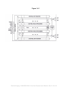
Shown on the following page is a block diagram of the Fairchild Imaging 2048 x 1 CMOS sensor.
Fairchild Imaging • CAM/CMOS-2K.LS Line Scan Camera User’s Manual • Rev C• 9 of 42


