


CV-L105
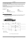
7.2. Configuration via I/F connector and jumpers
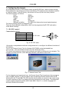
The binning function, pixel rate and RS-232C function can be controlled by TTL inputs on the
68pin Hirose interface connector and with jumper settings.
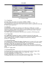
Below table describe the possible states of these inputs. Please refer to fig. 7. for principle.
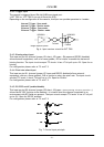
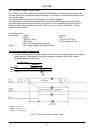
RS-232C contr. Binning Clock
Function
JP3
JP4
Pin
#30
JP1
JP2
Pin
#10
JP5
Pin
#31
Remarks
RS-232C control only O S H O O H O H
Factory setting. RS-232C enabled
L
#30 low for RS-232C enabled
RS-232C enable/disable
by I/F pin #30
S O
H
O O H O H
#30 high for RS-232C disabled
Binning fixed at 1024 by JP2 O S H
JP2 closed for 1024
H
#10 high for 2048
Binning select by I/F pin #10
S O H
S O
L
x H
#10 low for 1024
O
JP5 open for 30 MHz
Pixel clock select by JP5
S
H
JP5 closed for 15 MHz
H
#31 high for 30 MHz
Pixel clock select by I/F pin
#31
S O H x x H
O
L
#31 low for 15 MHz
RS-232C
disabled
Set by
jumper
& pin
O = jumper open
S = jumper short
H = input high. ( open. 5V by the internal 4.7 kΩ pull-up resistor)
L = input low. (closed to GND)
x = do not care
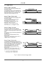
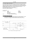
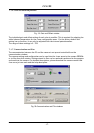
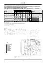
7.3. Potentiometers and jumpers placing
There are 5 solder jumpers on the main board (PK8234B), which are accessible for the user.
On the board (PK8235B) 7 potentiometers are found. The top one marked A/D is for factory
adjustment. Do not touch it.
The red, green and blue gain and offset potentiometers is factory adjusted to white color
balance at 3100K. It is used in factory setting configuration. As the green gain and offset is
reference, do not touch it.
JP4 JP5 JP2 P1 JP3
Top
A/D offset
R gain
R offset
G gain
G offset
B gain
B offset
Fig. 21. Potentiometers and jumpers placing
- 18 -