


– 5 –
ICX418AKL
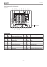
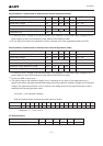
DC Characteristics
Output circuit supply current
Item
IDD
Symbol
5.0
Min. Unit RemarksTyp. Max.
mA10.0
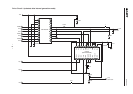
Bias Conditions 1 [when used in substrate bias internal generation mode]
Output circuit supply voltage
Reset drain voltage
Protective transistor bias
Substrate bias circuit supply voltage
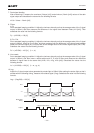
Substrate clock
∗1
VL setting is the VVL voltage of the vertical transfer clock waveform, or the same supply voltage as the VL
power supply for the V driver should be used. (When CXD1267AN is used.)
∗2
Do not apply a DC bias to the substrate clock pin, because a DC bias is generated within the CCD.
Item
VDD
VRD
VL
VDSUB
φSUB
Symbol
15.0
15.0
∗
1
15.0
∗
2
Min.
V
V
V
Unit
RemarksTyp. Max.
14.55
14.55
14.55
15.45
15.45
15.45
VRD = VDD
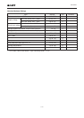
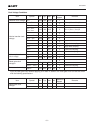
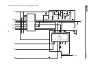
Bias Conditions 2 [when used in substrate bias external adjustment mode]
Output circuit supply voltage
Reset drain voltage
Protective transistor bias
Substrate bias circuit supply voltage
Substrate voltage adjustment range
Substrate voltage adjustment precision
∗3
VL setting is the VVL voltage of the vertical transfer clock waveform, or the same supply voltage as the VL
power supply for the V driver should be used. (When CXD1267AN is used.)
∗4
Connect to GND or leave open.
∗5
The setting value of the substrate voltage (VSUB) is indicated on the back of the image sensor by a
special code. When adjusting the substrate voltage externally, adjust the substrate voltage to the indicated
voltage. The adjustment precision is ±3%. However, this setting value has not significance when used in
substrate bias internal generation mode.
VSUB code — one character indication
Code and optimal setting correspond to each other as follows.
Item
VDD
VRD
VL
VDSUB
VSUB
∆VSUB
Symbol
15.0
15.0
∗
3
∗
4
Min.
V
V
V
%
Unit
RemarksTyp. Max.
14.55
14.55
6.0
–3
15.45
15.45
14.0
+3
VRD = VDD
∗
5
∗
5
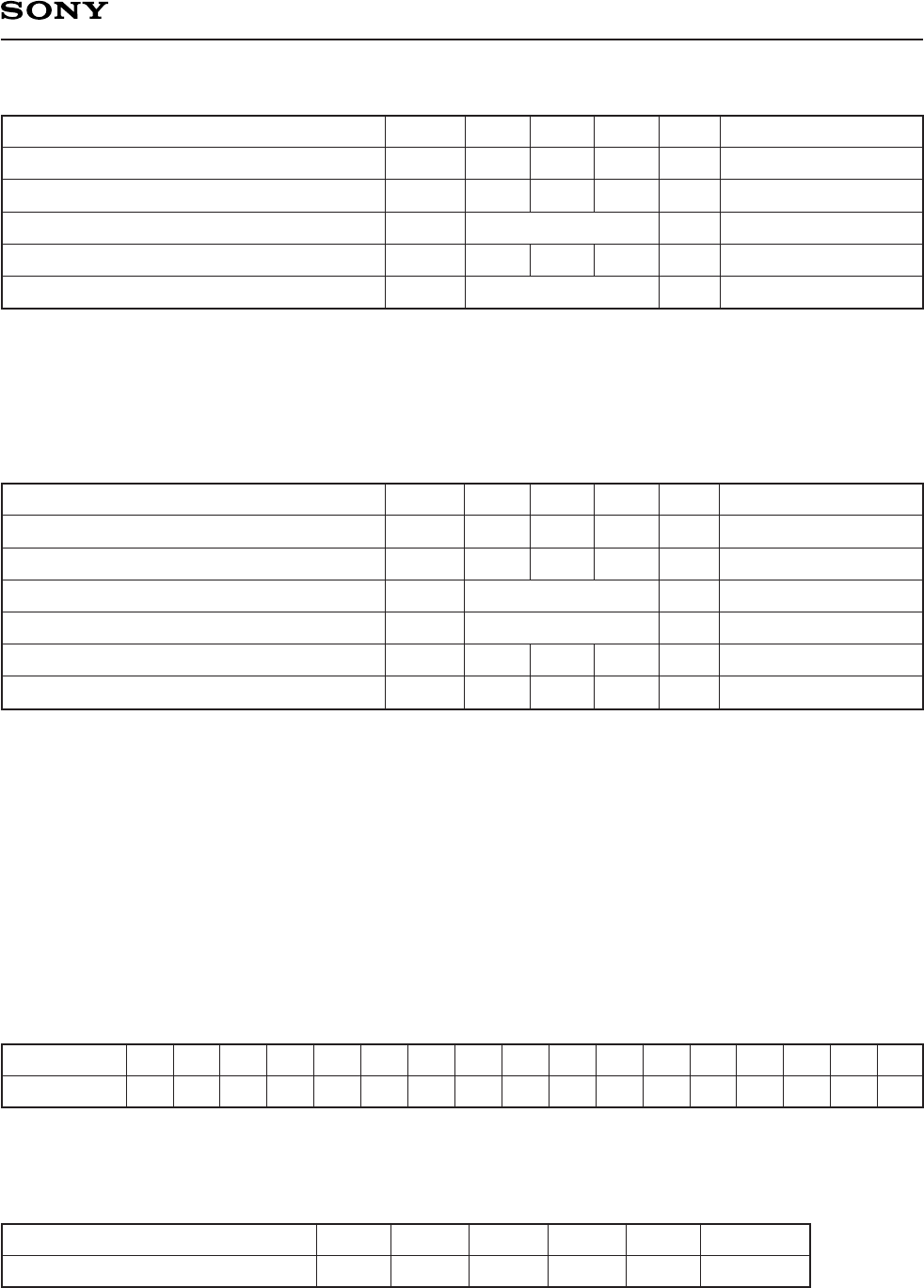
<Example> "L" → VSUB = 9.0V
VSUB code
Optimal setting
f
6.5
G
7.0
h
7.5
J
8.0
K
8.5
L
9.0
m
9.5
N
10.0
P
10.5
Q
11.0
S
12.0
U
13.0
V
13.5
W
14.0
R
11.5
T
12.5
E
6.0