


2002 Oct 23 10
Philips Semiconductors Product specification
40 Msps, 10-bit analog-to-digital
interface for CCD cameras
TDA8783
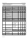
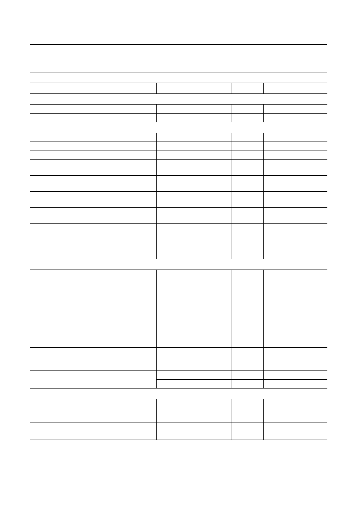
Clamps
g
m(ADC)
ADC clamp transconductance at clamp level − 7 − mS
g
m(CDS)
CDS clamp transconductance at clamp level − 1.5 − mS
Analog-to-Digital Converter (ADC)
f
CLK(max)
maximum clock frequency 40 −−MHz
t
CPH
clock pulse width HIGH 12 −−ns
t
CPL
clock pulse width LOW 12 −−ns
SR
CLK
clock input slew rate (rising and
falling edge)
10% to 90% 0.5 −−V/ns
V
i(ADC)(p-p)
ADC input voltage level
(peak-to-peak value)
− 2 − V
V
RB
ADC reference voltage output
code 0
− 1.5 − V
V
RT
ADC reference voltage output
code 1023
− 3.5 − V
I
ADCIN
ADC input current −2 − +120 µA
INL integral non-linearity ramp input −±0.6 ±1.5 LSB
DNL differential non-linearity ramp input −±0.2 ±0.75 LSB
t
d(s)
sampling delay time −−5ns
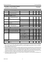
Total chain characteristics (CDS + AGC + ADC)
t
d
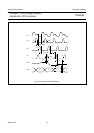
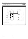
delay between SHD and CLK 50% at rising edges
CLK and SHD: transition full
scale code 0 to 1023;
f
cut(CDS)
= 120 MHz;
f
cut(AGC)
= 54 MHz;
V
i(CDS)
= 600 mV
− 30 − ns
N
tot(rms)
total output noise (RMS value) f
cut(CDS)
= 120 MHz;
f
cut(AGC)
= 40 MHz; note 2
G
AGC
= 4.5 dB − 0.125 − LSB
G
AGC
= 34.5 dB − 1.6 − LSB
V
offset(fl-d)
maximum offset between CCD
floating level and CCD dark pixel
level
−200 − +200 mV
V
n(i)(eq)(rms)
equivalent input noise voltage
(RMS value)
AGC gain = 34.5 dB − 125 −µV
AGC gain = 4.5 dB − 150 −µV
Digital-to-Analog Converter (OFDOUT)
V
OFDOUT(p-p)
additional 8-bit control DAC
(OFD) output voltage
(peak-to-peak value)
− 1.4 − V
V
OFDOUT(0)
DC output voltage for code 0 − 2.3 − V
V
OFDOUT(255)
DC output voltage for code 255 − 3.7 − V
SYMBOL PARAMETER CONDITIONS MIN. TYP. MAX. UNIT