


2002 Oct 23 8
Philips Semiconductors Product specification
40 Msps, 10-bit analog-to-digital
interface for CCD cameras
TDA8783
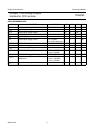
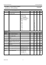
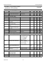
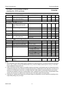
CHARACTERISTICS
V
CCA
=V
CCD
=5V; V
CCO
=3V; f
CLK
= 27 MHz; T
amb
=25°C; unless otherwise specified.
SYMBOL PARAMETER CONDITIONS MIN. TYP. MAX. UNIT
Supplies
V
CCA
analog supply voltage 4.75 5 5.25 V
V
CCD
digital supply voltage 4.75 5 5.25 V
V
CCO
digital outputs supply voltage 2.5 3 5.25 V
I
CCA
analog supply current − 78 95 mA
I
CCD
digital supply current − 18 20 mA
I
CCO
digital outputs supply current C
L
= 20 pF on all data
outputs; ramp input
− 1 − mA
Digital inputs
C
LOCK INPUT: CLK (REFERENCED TO DGND)
V
IL
LOW-level input voltage 0 − 0.8 V
V
IH
HIGH-level input voltage 2.0 − V
CCD
V
I
IL
LOW-level input current V
CLK
= 0.8 V −1 − +1 µA
I
IH
HIGH-level input current V
CLK
= 2.0 V −−20 µA
Z
i
input impedance f
CLK
= 27 MHz − 46 − kΩ
C
i
input capacitance f
CLK
= 27 MHz − 1 − pF
INPUTS: SHP AND SHD
V
IL
LOW-level input voltage 0 − 0.8 V
V
IH
HIGH-level input voltage 2.0 − V
CCD
V
I
IL
LOW-level input current V
IL
= 0.8 V −−6−µA
I
IH
HIGH-level input current V
IH
= 2.0 V − 0 −µA
INPUTS: SEN, SCLK, SDATA, OE, STDBY, CLPDM, CLPOB AND CLPADC
V
IL
LOW-level input voltage 0 − 0.8 V
V
IH
HIGH-level input voltage 2.0 − V
CCD
V
I
i
input current −2 − +2 µA
Correlated Double Sampling (CDS); note 1
V
i(CDS)(p-p)
CDS input amplitude pin 47
(peak-to-peak value)
− 400 1200 mV
I
CPCDS,
I
INP,
I
IND
input current pins 8, 46 and 47 −2 − +2 µA
t
CDS(min)
CDS control pulses minimum
active time
f
i(CDS1,2)
=f
CLK(pix)
;
V
i(CDS)(p-p)
= 600 mV
black-to-white transition in
1 pixel (±1 LSB typ.);
f
cut(CDS)
= 120 MHz;
f
cut(AGC)
= 54 MHz
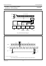
8 −−ns
t
hd1
hold time INP compared to control
pulse SHP
see Fig.5 − 1 − ns