


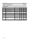
2002 Oct 23 11
Philips Semiconductors Product specification
40 Msps, 10-bit analog-to-digital
interface for CCD cameras
TDA8783
Notes
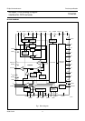
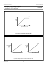
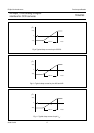
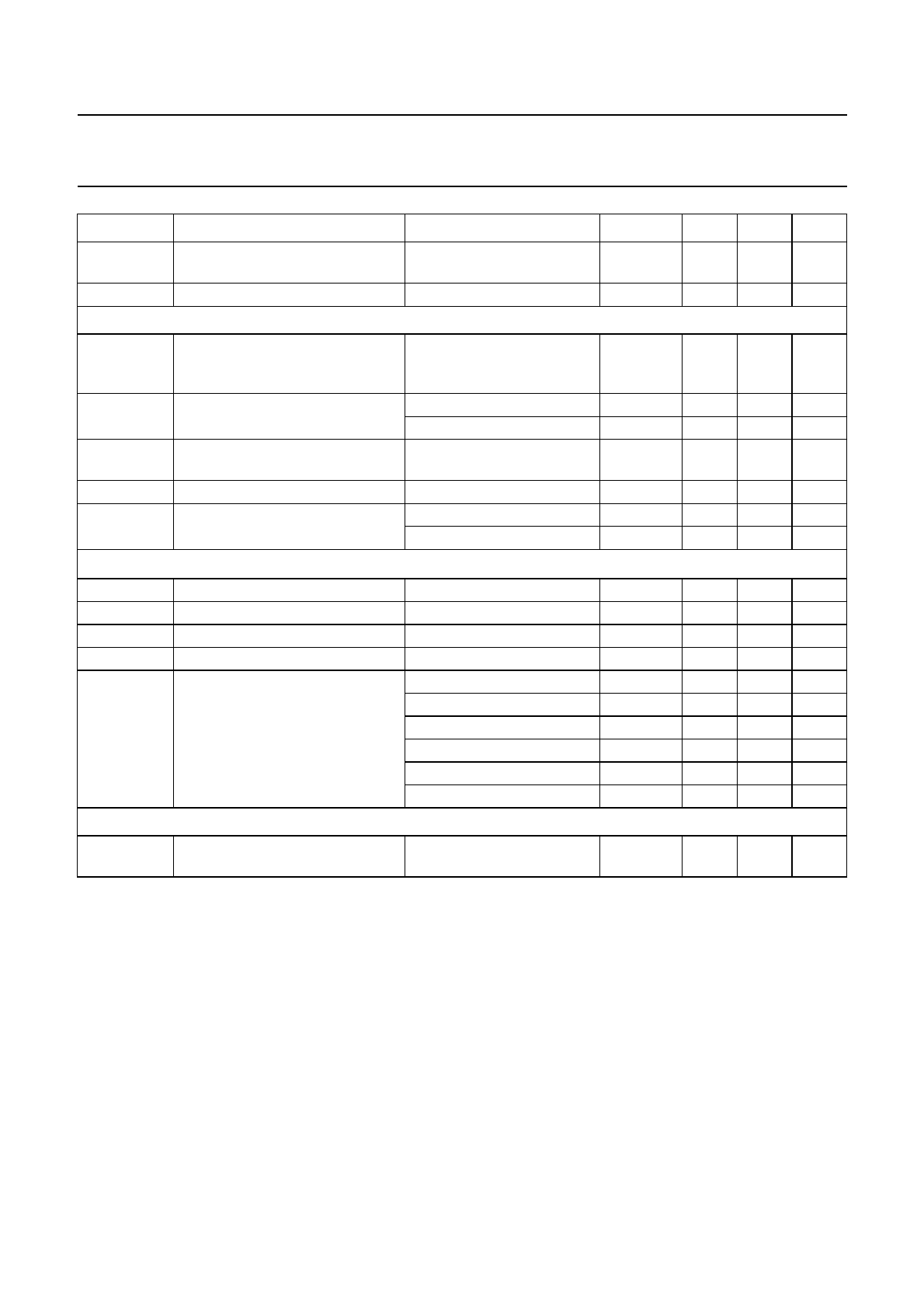
1. More information about CDS related signals is available in the following figures: The clamp current for pin CPCDS is
given in Fig. 9, clamp current for pins IND and INP in Fig 10 and for clamp current for pin V
ref
in Fig 11. The CDS
output amplitude is shown in Fig. 14
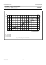
2. Noise measurement at ADC outputs: the coupling capacitor at the input is connected to ground, so that only the noise
contribution of the front-end is evaluated. The front-end operates at 18 Mpix with a line of 1024 pixels. The first 40 are
used to run CLPOB and the last 40 to run CLPDM. Data at the ADC outputs is measured during the other pixels.
The differences between the types of codes statistic is then computed; the result is the noise. No quantization noise
is taken into account as no signal is input. Figure15 gives noise figure graphs with signal input.
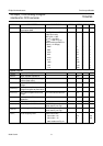
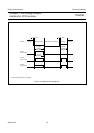
3. Depending on operating pixel frequency, the output voltage and capacitance must be determined according to the
output delay timings (t
o(d)
), see Fig.5.
Z
OFDOUT
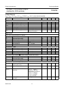
additional 8-bit control DAC
(OFD) output impedance
− 2000 −Ω
I
OFDOUT
OFD output current drive static −−50 µA
ADC clamp control DAC (see Fig.8)
V
DACOUT(p-p)
ADC clamp 10-bit control DAC
output voltage (peak-to-peak
value)
− 1 − V
V
DACOUT
DC output voltage code 0 − 1.5 − V
code 1023 − 2.5 − V
Z
DACOUT
ADC clamp control DAC output
impedance
−−250 Ω
I
DACOUT
DAC output current drive static −−50 µA
OFE
LOOP
maximum offset error of
DAC + ADC clamp loop
code 0 −±5−LSB
code 1023 −±5−LSB
Digital outputs (f
CLK
= 40 MHz; C
L
= 20 pF); note 3
V
OH
HIGH-level output voltage I
OH
= −1mA V
CCO
− 0.5 − V
CCO
V
V
OL
LOW-level output voltage I
OL
=1mA 0 − 0.5 V
I
OZ
output current in 3-state mode 0V<V
o
<V
CCO
−20 − +20 µA
t
o(h)
output hold time 8 −−ns
t
o(d)
output delay time C
L
= 20 pF; V
CCO
=5V − 17 23 ns
C
L
= 10 pF; V
CCO
=5V − 15 21 ns
C
L
= 20 pF; V
CCO
=3V − 20 29 ns
C
L
= 10 pF; V
CCO
=3V − 17 25 ns
C
L
= 20 pF; V
CCO
= 2.5 V − 22 33 ns
C
L
= 10 pF; V
CCO
= 2.5 V − 18 28 ns
Serial interface
f
SCLK(max)
maximum frequency of serial
interface
5 −−MHz
SYMBOL PARAMETER CONDITIONS MIN. TYP. MAX. UNIT