


Philips Semiconductors
TDA9964
12-bit, 3.0 V, 30 Msps analog-to-digital interface for CCD cameras
Objective specification Rev. 03 — 16 January 2001 14 of 23
9397 750 07918
© Philips Electronics N.V. 2001. All rights reserved.
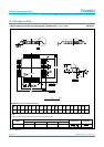
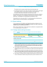
Table 7: Serial interface programming
Address bits Data bits D9 to D0
A3 A2 A1 A0
0 0 0 0 PGA gain control (SD7 to SD0)
0001DAC OFDOUT output control (SD7 to SD0)
0 0 1 0 ADC clamp reference control (SD6 to SD0); from code 0 to 127
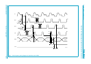
0 0 1 1 control pulses (pins SHP, SHD, CLPDM, CLPOB, BLK and CLK)
polarity settings; SD2, SD6, SD7 and SD9 should be set to logic 1;
for SD6 and SD7 see Ta ble 9 , 10, 11, and 12
0 1 0 0 SD7 = 0 by default; SD7 = 1 PGA gain up to 36 dB but noise and
clamp behaviour are not guaranteed
1 1 1 1 initialization (SD11 to SD0 = 0)
other addresses test modes
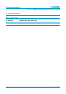
Table 8: Polarity settings
Symbol Pin Serial control bit Active edge or level
SHP and SHD 45 and 46 SD4 1 = HIGH; 0 = LOW
CLK 47 SD5 1 = rising; 0 = falling
CLPDM 48 SD0 1 = HIGH; 0 = LOW
CLPOB 44 SD1 1 = HIGH; 0 = LOW
BLK 43 SD3 1 = HIGH; 0 = LOW
VSYNC 20 SD8 0 = rising; 1 = falling
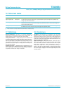
Table 9: Standby control using pin STDBY
Bit SD7 of
register 0011
STDBY ADC digital outputs
D11 to D0
I
CCA
+I
CCO
+I
CCD
(typ.)
1 1 last logic state 1.5 mA
0 active 65 mA
0 1 active 65 mA
0 test logic state 1.5 mA
Table 10: Output enable selection using output enable pin (
OE)
Bit SD6 of register 0011 OE ADC digital outputs D11 to D0
1 0 active, binary
1 high impedance
0 0 high impedance
1 active binary
Table 11: Standby control by serial interface (register
address A3 = 0, A2 = 0, A1 = 1 and A0 = 1); pin STDBY connected to ground
SD7 ADC digital outputs D11 to D0 I
CCA
+I
CCO
+I
CCD
(typ.)
0 last logic state 1.5 mA
1 active 65 mA