


Philips Semiconductors
TDA9964
12-bit, 3.0 V, 30 Msps analog-to-digital interface for CCD cameras
Objective specification Rev. 03 — 16 January 2001 8 of 23
9397 750 07918
© Philips Electronics N.V. 2001. All rights reserved.
f
pix(min)
minimum pixel frequency tbf −−MHz
t
CLKH
CLK pulse width HIGH 12 −−ns
t
CLKL
CLK pulse width LOW 12 −−ns
t
d(SHD;CLK)
time delay between
SHD and CLK
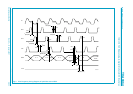
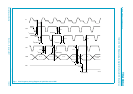
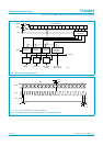
see Figure 3 and 4 10 −−ns
t
su(BLK;SHD)
set-up time of BLK compared
to SHD
see Figure 3 and 4 5 −−ns
V
i(IN)
video input dynamic signal
for ADC full-scale output
PGA code = 00 800 −−mV
PGA code = 255 50 −−mV
N
tot(rms)
total noise from CDS input to
ADC output (RMS value)
see Figure 8
PGA gain = 0 dB − 1.5 − LSB
PGA gain = 9 dB − 2.2 − LSB
E
in(rms)
equivalent input noise
voltage (RMS value)
PGA gain = 24 dB − 70 −µV
PGA gain = 9 dB − 140 −µV
O
CCD(max)
maximum offset between
CCD floating level and CCD
dark pixel level
−100 − +100 mV
Digital-to-analog converter (OFDOUT DAC)
V
OFDOUT(p-p)
additional 8-bit control DAC
(OFD) output voltage
(peak-to-peak value)
R
i
=1MΩ−1.0 − V
V
OFDOUT(0)
DC output voltage for code 0 − AGND − V
V
OFDOUT(255)
DC output voltage for
code 255
− AGND + 1.0 − V
TC
DAC
DAC output range
temperature coefficient
− 250 − ppm/°C
Z
OFDOUT
DAC output impedance − 2000 −Ω
I
OFDOUT
OFD output current drive static −− 100 µA
Digital outputs (f
pix
= 30 MHz; C
L
= 10 pF); see Figure 3 and 4
V
OH
HIGH-level output voltage I
OH
= −1mA V
CCO
− 0.5 − V
CCO
V
V
OL
LOW-level output voltage I
OL
=1mA 0 − 0.5 V
I
OZ
output current in 3-state
mode
0.5 V < V
o
<V
CCO
−20 − +20 µA
t
h(o)
output hold time 5 −−ns
t
d(o)
output delay time C
L
= 10 pF; V
CCO
= 3.0 V − 12 tbf ns
C
L
= 10 pF; V
CCO
= 2.7 V − 14 tbf ns
C
L
output load capacitance −− 15 pF
Serial interface
f
SCLK(max)
maximum frequency of serial
interface
10 −−MHz
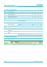
Table 6: Characteristics
…continued
V
CCA
=V
CCD
= 3.0 V; V
CCO
= 2.7 V; f
pix
= 30 MHz; T
amb
=25
°
C; unless otherwise specified.
Symbol Parameter Conditions Min Typ Max Unit