30 Advanced Camera Operation Manual
A thin layer of silicon dioxide is grown on a section of silicon and a conductive
gate structure is applied over the oxide. Applying a positive electrical potential
to the gate creates a depletion region where the free electrons generated by
incoming photons can be stored. A potential well collects electronic charge from
any source until the well is filled. Practical potential well capacities range up to a
million electrons. Depletion depths range from a few micrometers up to tens of
micrometers in specially prepared silicon.
Electrons freed by thermal agitation and by high-energy particles are
indistinguishable from those generated by photon interaction. These dark
electrons can have an adverse effect on the detection limits for photon-induced
charge.
Charge Transfer
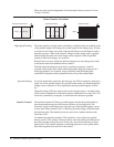
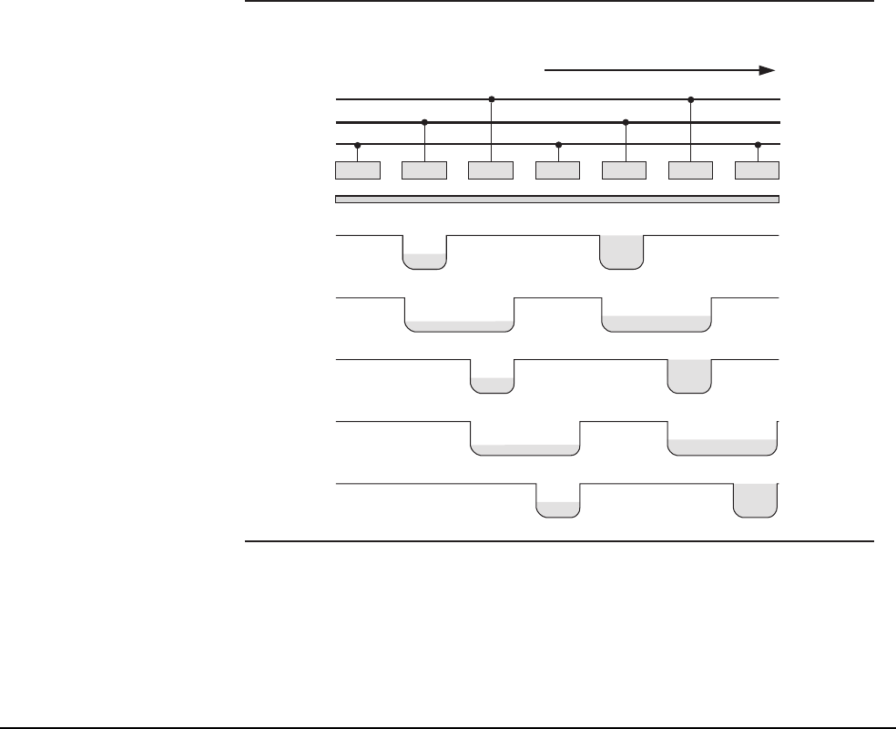
The charge collected in a potential well must be brought to an output amplifier.
When a series of oxide and conductive gate structures is fabricated with
multiple phases, potential wells can be propagated through a silicon sheet.
This charge transfer concept is essential to understanding charge-coupled
devices. When an appropriate sequence of potentials is applied to the gates, the
potential wells are propagated in the direction shown in the figure Charge
Transfer. Any charge that has been collected is carried along in the wells, and the
charge packets in each potential well remain separated. Charge packets can be
transferred thousands of times without significant loss of charge.
Charge Transfer
Phase 1
Phase 2
Phase 3
Gate
Direction of Charge Transfer
Q
2
Q
2
Q
2
Q
2
Q
2
Q
1
Q
1
Q
1
Q
1
Q
1
t
2
t
3
t
4
t
0
t
1
layerSiO
2
The illustration is simplified to emphasize the concept. To ensure effective
charge transfer, charge propagation actually occurs in a channel buried just
below the surface, where there is no interference from interface states. The gates
actually overlap, to create the drift field required for efficient charge transfer.


