32 Advanced Camera Operation Manual
CCD Readout
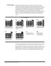
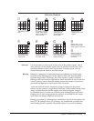
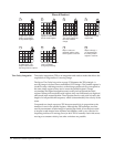
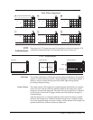
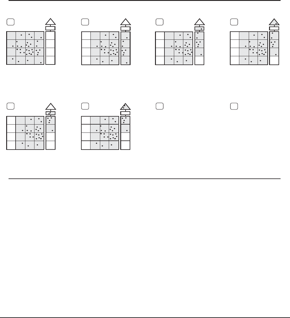
The standard CCD readout sequence is shown in CCD Readout. After an
integration, a programmed sequence of changing gate potentials causes all
charge packets stored in the parallel register to be shifted one pixel towards the
serial register; the first charge packet in each column is shifted into the serial
register. Once in the serial register, charge packets are individually shifted
toward the output amplifier. The output amplifier produces a signal
proportional to the charge in each packet. After the serial register is emptied of
charge, a second row of charge packets is shifted in from the parallel register.
The process continues until all charge has been shifted out of the parallel
register.
8
1
2
4
3
Charge in the parallel
register is shifted one
row. The first row is
shifted into the serial
register.
CCD Readout
The CCD is exposed
to light and a charge
pattern accumulates
in the parallel register.
The first pixel is serially
shifted into the output
node.
The charge at the out-
put node is collected
for signal processing.
Steps 2 through 7
are repeated until
the entire parallel
register is read out.
Steps 5 and 6 are re-
peated until the entire
serial register is read out.
The charge from the
next pixel is shifted
to the output node.
The charge at the out-
put node is collected
for signal processing.
5
6
7
All CCD imagers depend on the efficient transport of charge from the photosites
to the output amplifier. Because the charge from wells located far from the
output amplifier must undergo many hundreds of transfers, the charge transfer
efficiency (CTE) is important. A scientific-grade CCD imager exhibits a CTE of
0.99999, where 1.0 is perfect. CTE is of special concern at low charge levels
where a small loss of charge can cause significant degradation of the image.


