


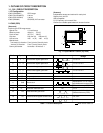
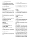
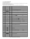
Pin 1
2
8
34
2
H
V
Pin 9
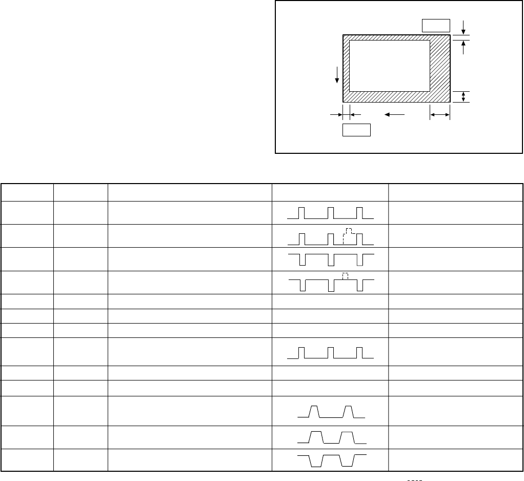
Fig. 1-1.Optical Black Location (Top View)
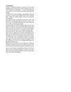
Pin No.
1
Symbol
2
3
4
5, 6, 7, 10
8
9
12
13
14
15
16
V
3
V 1
GND
OS
OD
O
SUB
PL
RS
H1
H2
Pin Description
Vertical shift register gate clock
Vertical shift register gate clock
Vertical shift register gate clock
Vertical shift register gate clock
Horizontal shift register transfer clock
Board bias
Reset transister gate clock
Horizontal shift register transfer clock
GND
Image output
Output transister drain
Protection transistor bias
Waveform
DC
Voltage
-7.5 V, 0 V
-7.5 V, 0 V, 15 V
-7.5 V, 0 V
-7.5 V, 0 V, 15 V
Amplitude 22.5 V Ex. 6 V (Bias
level is different from every CCD)
-7.5 V
0 V, 3.5 V
0 V, 3.5 V
Table 1-1. CCD Pin Description
DC
15 V
When sensor read-out
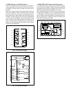
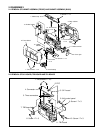
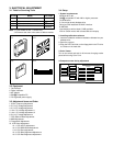
1. OUTLINE OF CIRCUIT DESCRIPTION
1-1. CA-1 CIRCUIT DESCRIPTION
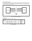
1. IC Configuration
IC903 (ICX204AK) CCD imager
IC902 (74VHC04MTC) H driver
IC904 (CXD1267AN) V driver
IC905 (AD9802) CDS/AGC, A/D converter
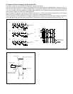
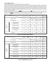
2. IC903 (CCD)
[Structure]
Interline type CCD image sensor
Optical size 1/3 inch format
Effective pixels 1034 (H) 779 (V)
Pixels in total 1077 (H) 788 (V)
Chip size 5.80 mm (H) 4.92 mm (V)
Unit cell size 4.65 m (H) 4.65 m (H)
Optical black
Horizontal (H) direction: Front 3 pixels, Rear 40 pixels
Vertical (V) direction: Front 7 pixels, Rear 2 pixels
Dummy bit number Horizontal : 29 Vertical : 1
V
2B
Amplitude 3.5 V Ex. 5 V, 10 V
(Different from every CCD)
V 2A
[Features]
Independent storage and retrieval for each pixel
Square pixel unit cell
XGA compatible
R, G, B primary color mosaic filter
Continuous variable speed electronic shutter function
11 SUB Board clock
(Different from every CCD) Ex. 6V