


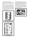
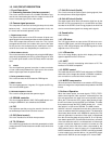
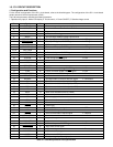
1A
1
1Y
2
2A
3
2Y
4
3A
5
3Y
6
GND
7
4Y
8
4A
9
5Y
10
5A
11
6Y
12
6A
13
V
CC
14
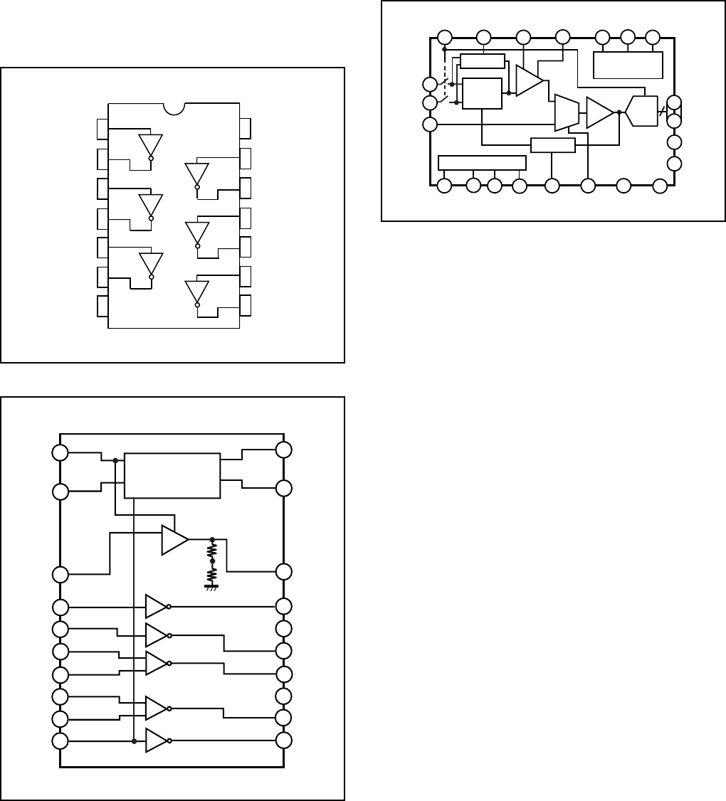
Fig. 1-2. IC902 Block Diagram
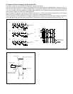
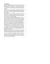
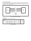
1
18
10
9
8
7
6
5
4
3
2
14
15
16
17
20
19
11
12
13
CPP1
CPP2
DC OUT
VSHT
V
1
VL
V 2
V 4
VM
V 3
XV4
CPP3
VH
DCIN
XSHT
XV2
XV1
XSG1
XV3
XSG2
Change Pump
Fig. 1-3. IC904 Block Diagram
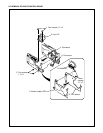
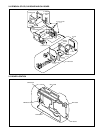
3. IC902 (H Driver) and IC904 (V Driver)
An H driver (IC902) and V driver (IC904) are necessary in
order to generate the clocks (vertical transfer clock, horizon-
tal transfer clock and electronic shutter clock) which driver
the CCD.
IC902 is an inverter IC which drives the horizontal CCDs (H1
and H2). In addition the XV1-XV4 signals which are output
from Pins (166), (167), (169) and (171) of IC102 are the ver-
tical transfer clocks, and the XSG1 and XSG2 signals which
is output from Pins (168) and (170) of IC102 is superimposed
onto XV1 and XV3 at IC904 in order to generate a ternary
pulse. In addition, the XSUB signal which is output from Pin
(165) of IC102 is used as the sweep pulse for the electronic
shutter, and the RG signal which is output from Pin (159) of
IC102 is the reset gate clock.
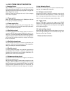
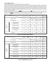
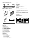
4. IC905 (CDS, AGC Circuit and A/D converter)
The video signal which is output from the CCD is input to
Pins (26) and (27) of IC905. There are S/H blocks inside IC905
generated from the XSHP and XSHD pulses, and it is here
that CDS (correlated double sampling) is carried out.
After passing through the CDS circuit, the signal passes
through the AGC amplifier. It is A/C converted internally into
a 10-bit signal, and is then input to IC102 of the CA2 circuit
board. The gain of the AGC amplifier is controlled by the volt-
age at pin (29) which is output from IC102 of the CA2 circuit
board and smoothed by the PWM.
Fig. 1-4. IC905 Block Diagram
27
29
36
26
16
22
21
30
2319
11
12
17
PBLK
A/D
ACVDD
CMLEVEL
VRT
VTB
STBY CLPOB
ADCMODE
TIMING
GENERATOR
CLPDM PGACONT1
PGACONT2
SHP
SHD ADCCLK
PIN
DIN
ADCIN
DOUT
DRVDD
DVDD
ADVDD
2
37 20
18
47
48
43
3341
CLAMP
REFERENCE
CLAMP
CDS
PGA
MUX S/H
AD9802
10