


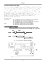
CV-A1
5.3. Input and Output Circuits
In the following schematic diagrams the input and output circuits for video and timing signals
are shown. For alternative connections refer to “7.4. Internal Switch and Jumper Settings.”
Jumper settings are shown as for factory default.
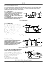
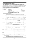
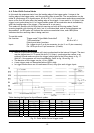
5.3.1. Video output
300 mV
500 mV
GND
#4/12
75
Video
Output
NC
CXA1310
32
BNC
300 mV
500 mV
300 mV
500 mV
GND
#4/12
75
Video
Output
NC
CXA1310
32
BNC
GND
#4/12
75
Video
Output
NC
CXA1310
32
BNC
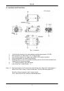
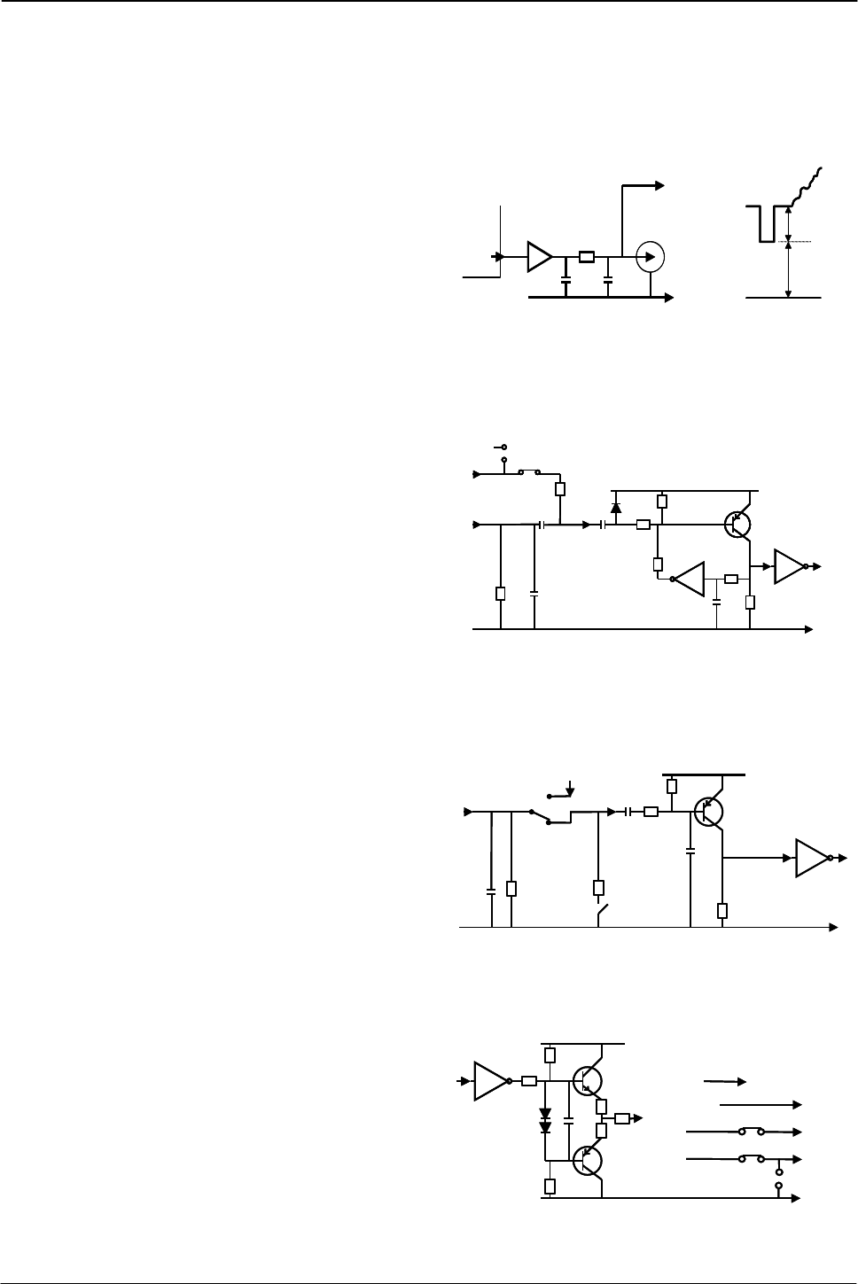
The video output is a 75 Ω DC coupled circuit.
The BNC connector and pin #4 on the 12-pin
connector is in parallel. Avoid double
termination. The video DC level is shown with
75 Ω termination.
In the composite signal, there are no equalize
and serration pulses in the vertical sync.
Fig. 4. Video output.
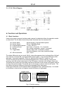
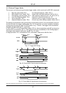
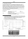
5.3.2. Trigger input
+12v
GND
+5V
33k
TTL
1k
GND
100n
1k
Trigger
input
33k
100k
1n
NC
1k
#5/6
JP4#11/12
100
JP1
+12v
GND
+5V
33k
TTL
1k
GND
100n
1k
Trigger
input
33k
100k
1n
NC
1k
#5/6
JP4#11/12
100
JP1
GND
+5V
33k
TTL
1k
GND
100n
1k
Trigger
input
33k
100k
1n
NC
1k
#5/6
JP4#11/12
100
JP1
The trigger input is AC coupled. To allow a
long pulse width, the input circuit is a flip
flop, which is toggled by the negative or
positive differentiated spikes caused by the
falling or rising trigger edges.
The trigger polarity can be changed.
Trigger input level 4 V ±2 V.
The trigger-input impedance is 1 kΩ.
JP1 and JP4 are for alternative
configuration for pin #10.
Fig. 5. Trigger input.
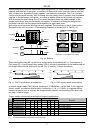
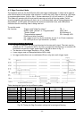
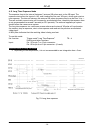
+5V
47p
33k
TTL
1k2
GND
10µ
4k7
VD HD
Input/output
+
75
SW2
1k
1n
From VD HD
output
SW1
+5V
47p
33k
TTL
1k2
GND
10µ
4k7
VD HD
Input/output
+
75
SW2
1k
1n
From VD HD
output
SW1
5.3.3. HD and VD input
The input circuit for external HD and VD
signals are shown. It can be 75 Ω
terminated by closing SW2. SW1 will switch
to output the internal HD and VD signal.
HD and VD input level is 4 V ±2 V.
Fig. 6. HD and VD input.
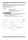
5.3.4. HD, VD, PCLK, WEN and EEN output
Output circuit for these signals are 75 Ω
complementary emitter followers. It will
deliver a full TTL signal. JP5 and JP3 are for
alternative configuration for pin #10.
GND
+5V
10
10
10k
10k
67
TTL
220
VD, HD
WEN/ EEN
PCLK
WEN
#10/12
#6/6
#9/12
SW1
JP3
JP2
JP5
GND
+5V
10
10
10k
10k
67
TTL
220
VD, HD
WEN/ EEN
PCLK
WEN
#10/12
#6/6
#9/12
SW1
JP3
JP2
JP5
Output level ≥4 V from 75Ω. (No
termination).
The WEN polarity can be changed.
Signal on pin #6/6 can be changed.
Fig. 7. HD, VD, PCLK, WEN and EEN output.
- 5 -
JPT 08-10-03: 11:01