


CV-A33CL
- 8 -
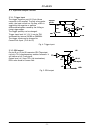
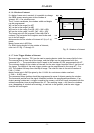
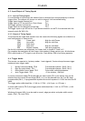
6.1.3. Column Process
The voltage signal from a single pixel is send to the
column amplifier trough the 4 to 1 multiplexer. After
the S/H circuit, the offset and gain calibrating is
perform. A 10 bit A/D converter send the digital pixel
signal to the digital horizontal shift register by a 1 to 4
multiplexing. Signals from a single row with 667 pixels
are processed in parallel and send to the shift register.
A/DS/H
Columns
10 bit
video
To shift
Register
through
1 to 4
multiplex
Amp
Offset
Gain
calibr
Control and timing
A/DS/H
Columns
10 bit
video
To shift
Register
through
1 to 4
multiplex
Amp
Offset
Gain
calibr
Control and timing
Control and timing is done from the timing block.
Fig. 9. Column processing principle
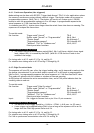
The calibrate command CB = 0 will start an automatic
calibrate routine for offset and gain for all 167 A/D
converter. It reduces the vertical fix pattern column noise.
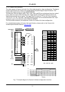
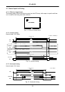
667 x 10 bit register
4 to 1 multiplexer
167 x A/D converter
1 to 4 multiplexer
667 x 502 sensor array
659 x 494 Active pixels
667 Columns
502
Rows
Row decode
Timing
10 bit digital
Video out
(1,1)
(502,667)
8 rows and 8 columns
optical dark pixels
667 x 10 bit register
4 to 1 multiplexer
167 x A/D converter
1 to 4 multiplexer
667 x 502 sensor array
659 x 494 Active pixels
667 Columns
502
Rows
Row decode
Timing
10 bit digital
Video out
(1,1)
(502,667)
8 rows and 8 columns
optical dark pixels
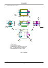
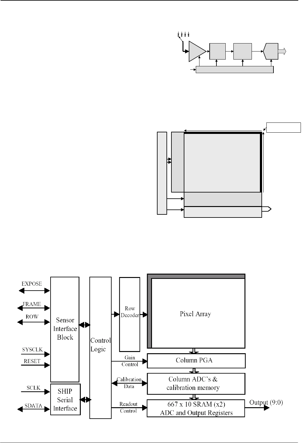
6.1.4. CV-A33 CMOS Sensor array
The CMOS sensor total array is 667 (h) x 502 (v).
Here the 659 (h) x 494 (v) is active photo sensing
pixels. 8 pixels (h) and 8 rows (v) are optical
black pixels for internal black level reference.
There is an A/D converter for each 4 columns.
A 4 to 1 multiplexer feed the signals from 4
columns to a A/D converter. The digital
converter output is multiplexed to the 667 x10
bit register.
Fig. 10. CV-A33 CMOS sensor array
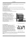
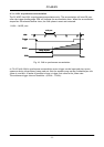
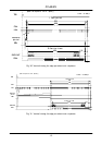
6.1.5. CMOS Sensor principle diagram
Fig. 11. CMOS sensor principle diagram