


– 10 –
ICX274AQ
∗
1
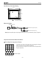
When two vertical transfer clock drivers CXD3400N are used.
∗
2
tf ≥ tr – 2ns, and the cross-point voltage (VCR) for the Hφ1β (β = A, B) rising side of the Hφ1β and Hφ2β
waveforms must be VφH/2 [V] or more.
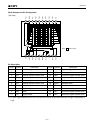
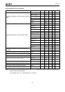
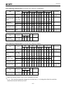
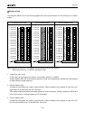
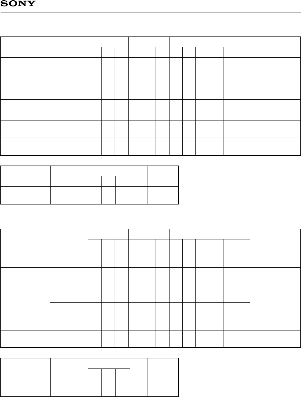
Clock Switching Characteristics (Horizontal drive frequency: 28.6364MHz)
Min.
twh
Typ. Max.Min. Typ. Max.Min. Typ. Max. Min. Typ. Max.
twl tr tf
3.3
10
10
4
3.5
12.5
12.5
7
2.1
10
10
12.5
12.5
24
0.5
5
5
2
7.5
7.5
0.5
15
0.5
5
5
3
400
7.5
7.5
0.5
Unit
µs
ns
ns
ns
µs
Remarks
During
readout
∗
1
∗
2
During drain
charge
Item
Readout clock
Vertical transfer
clock
Horizontal
transfer clock
Reset gate clock
Substrate clock
Symbol
VT
Vφ1, Vφ4,
Vφ2α, Vφ3α
(α = A to C)
Hφ1β (β = A, B)
Hφ2β (β = A, B)
φRG
φSUB
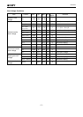
Min.
two
Typ. Max.
810
Unit
ns
RemarksItem
Horizontal
transfer clock
Symbol
Hφ1A, Hφ1B,
Hφ2A, Hφ2B
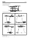
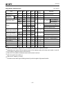
Clock Switching Characteristics (Horizontal drive frequency: 36MHz)
Min.
twh
Typ. Max.Min. Typ. Max.Min. Typ. Max. Min. Typ. Max.
twl tr tf
4.0
8
8
4
4.2
9
9
5.5
1.67
8
8
9
9
8
0.5
5
5
2
6
6
0.25
15
0.5
5
5
3
400
6
6
0.25
Unit
µs
ns
ns
ns
µs
Remarks
During
readout
∗
1
∗
2
During drain
charge
Item
Readout clock
Vertical transfer
clock
Horizontal
transfer clock
Reset gate clock
Substrate clock
Symbol
VT
Vφ1, Vφ4,
Vφ2α, Vφ3α
(α = A to C)
Hφ1β (β = A, B)
Hφ2β (β = A, B)
φRG
φSUB
Min.
two
Typ. Max.
89
Unit
ns
RemarksItem
Horizontal
transfer clock
Symbol
Hφ1A, Hφ1B,
Hφ2A, Hφ2B