


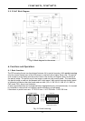
CV-M4
+
/M4
+
CL, CV-M7
+
/M7
+
CL
- 5 -
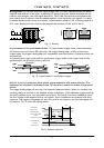
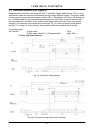
5.3. Digital Output Connector for Camera Link
This pin configuration is only valid for CV-M4
+
CL and CV-M
+
7CL
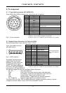
Pin no. Signal Function Remarks
1 14 Shield Shield
2 15 -/+ TX0
2 16 -/+ TX1
4 17 -/+ TX2
Video signal, LEN, FEN,
DVAL and EEN
Multiplexed signals
5 18 -/+ TXCLK Pixel clock
6 19 -/+ TX3 Video, LEN, FEN, DVAL, EEN
Multiplexed signals
7 20 +/- STC RXD in
8 21 -/+ STFG TXD out
Or via pin #6 # 7 12pin
if JP 301 open
9 22 -/+ TRIG Trigger input
*1) Or TTL on #10 12 pin
10 23 -/+ Multi Multiple exposure
*1) Or TTL on #11 12 pin
11 24
12 25
13 26 Shield Shield
*1) input on 12-pin con. or LVDS/(CL) by command TP or int. SW301-1
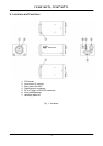
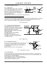
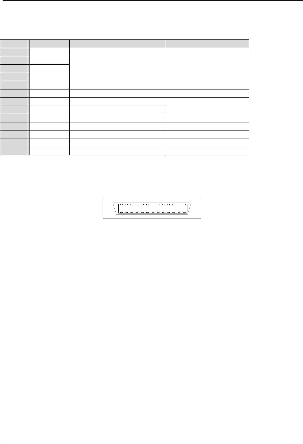
Type: 26 pin MRD connector
3M 10226-1A10JL
13
14
1
26
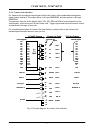
Fig. 4. Camera Link connector
The digital output signals follow the Camera Link standardized multiplexed signal output
interface. The output driver is NS type DS90CR283, and the receiver is NS type DS90CR284.
The following signals are found on the Digital Output Connector:
SerTC RXD serial data to camera
SerTFG TXD serial data to frame grabber
CC1 Trigger signal in for exposure control.
CC2 Trigger input for multiple exposure
X0 to X3 Camera Link multiplexed data out
Xclk Camera Link clock. Used as pixel clock.
In the Channel Link X0 to X3 multiplexed signals the following signals are encoded.
D0 – D9 10 bit video data out
LEN Line ENable. A pulse for the beginning of a new line.
FEN Frame ENable. Video frame data is valid.
DVAL Data VALid.
EEN Exposure Enable.
The polarity for LEN, FEN and Multi is positive and TRIG in negative as factory setting. It can be
changed by internal SW301-2 and 3 or RS 232C command FP and TP.
For Camera Link interface principle diagram please check Fig. 8.