


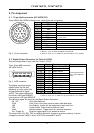
CV-M4
+
/M4
+
CL, CV-M7
+
/M7
+
CL
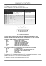
5.4. Input and Output Circuits
GND
#4/12
75
Video
Output
NC
68p
1µ2
L
500 mV
GND
Black
level
GND
#4/12
75
Video
Output
NC
68p
1µ2
L
500 mV
GND
Black
level
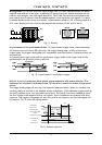
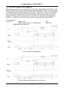
5.4.1. Video output
The analogue video output without composite
sync is a 75 Ω DC coupled circuit. It is for test
only. It can be used for iris control if the
camera is in normal mode. The video black level
is 0.5 volt without termination. The video is
without composite sync.
Analogue video in partial scan is only valid for the scanned area.
Important note on using this signal for iris control.
The signal for iris video output is taken from the video signal after the gain control. If it is used
for auto iris control, the digital output video level can only be adjusted with the lens level
adjust. The camera gain adjust will only change the working point.
Fig. 5. Video output.
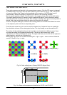
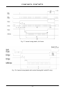
5.4.2. Trigger input Multi Shutter input
GND
+5V
15k
TTL
1k
GND
100n
1k
68k
100k
1n
10k
Trig input pin #10
Multi shut pin #11
GND
+5V
15k
TTL
1k
GND
100n
1k
68k
100k
1n
10k
Trig input pin #10
Multi shut pin #11
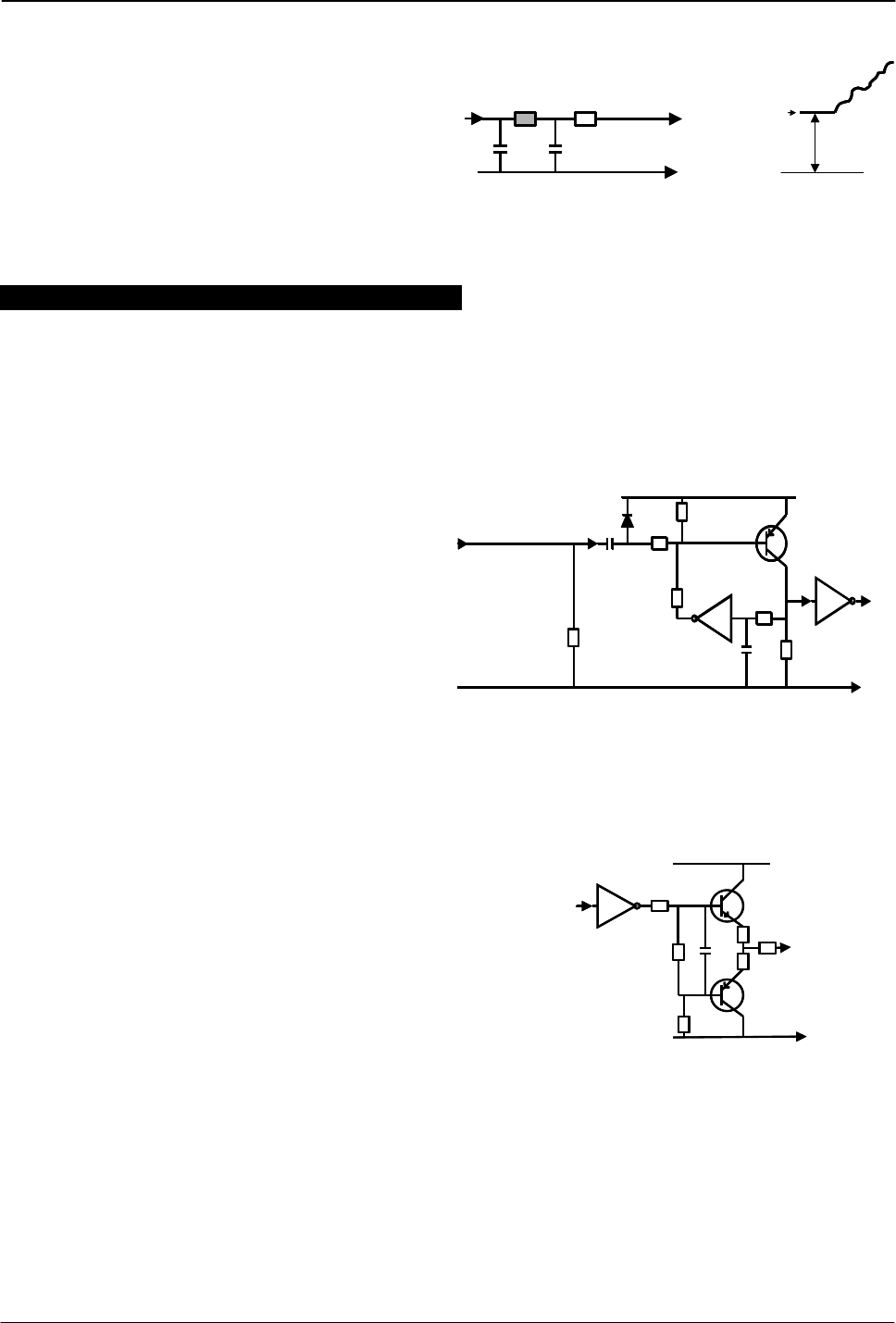
The trigger inputs on the 12 pin Hirose
connector is AC coupled. To allow a long pulse
width, the input circuit is a flip flop, which is
toggled by the negative or positive
differentiated spikes caused by the falling or
rising trigger edges.
The trigger polarity can be changed.
Trigger input level 4 V ±2 V.
The trigger-input impedance is 10 kΩ.
The trigger inputs can be changed to LVDS
or Camera Link input.
Fig. 6. Trigger input.
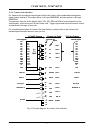
GND
+5V
2
2
10k
2k2
75
TTL
100
#9/12
Sync. out
GND
+5V
2
2
10k
2k2
75
TTL
100
#9/12
Sync. out
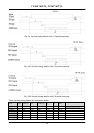
5.4.3. Composite Sync output
On pin #9 on 12 pin HR connector EEN or composite sync
can be output. (Command SE). The output circuit is 75
Ω complementary emitter followers. It will deliver a
full 5 volt signal.
Output level ≥4 V from 75Ω. (No termination).
Fig. 7. Composite Sync. output
5.4.4. LVDS interface
For LVDS the digital input and output signals follow the EIA 644 standard. It is also called Low
Voltage Differential Signal (LVDS). The output differential line driver is NS type DS90C031, and
the line receiver is NS type DS90C032.
Typical LVDS output level is ±350 mVolt differential.
Typical LVDS input threshold is ±100 mVolt differential.
Typical LVDS line impedance is 100 Ω.
- 6 -