


7 - 6 C156-E097-01EN
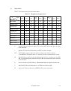
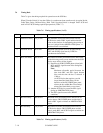
Table 7.1 INFORMATION TRANSFER phase identification
C/D I/O MSG DB7-0, P Direction Phase
0
0
1
1
0
0
1
1
0
1
0
1
0
1
0
1
0
0
0
0
1
1
1
1
Data
Data
Command (CDB)
Status
–
–
Message
Message
INIT → TARG
INIT ← TARG
INIT → TARG
INIT ← TARG
–
–
INIT → TARG
INIT ← TARG
DATA OUT
DATA IN
COMMAND
STATUS
not used
not used
MESSAGE OUT
MESSAGE IN
7.3 Electrical Requirements
7.3.1 SCSI interface
(1) Driver and receiver
For the interface signal driver, an open-collector or tri-state buffer circuit that satisfies the
following output characteristics is used. All signals are negative logic (true = "L").
The receiver and non-driver of the SCSI device under the power-on state should satisfy the
following input characteristics on each signal.
Output characteristics
V
OL
= 0.0 to 0.50 VDC (@ I
OL
= 48 mA)
V
OH
= 2.5 to 5.25 VDC
Input characteristics
V
IL
= 0.0 to 0.80 VDC
I
IL
= –0.4 to 0.0 mA (@ V
I
= 0.5 VDC)
V
IH
= 2.0 to 5.25 VDC
I
IH
= 0.0 to 0.1 mA (@ V
I
= 2.7 VDC)
Input hysteresis = 0.2 VDC min.
Input capacitance = 25
P
F max.
Note:
The SCSI device under the power-off state should satisfy the characteristics of I
IL
and I
IH
.
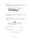
Recommended circuit
Driver: MB463 (Fujitsu) or SN7438 (TI) (Open-collector NAND gate)
Receiver: SN74LS240 or SN74LS19 (TI) (Schmitt trigger input inverter)