


25
MZ-R501/R501PC
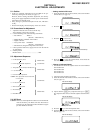
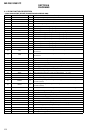
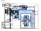
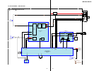
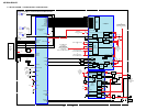
• IC801 CXD2671-204GA (SYSTEM CONTROLLER, DIGITAL SIGNAL PROCESSOR, 16M BIT D-RAM)
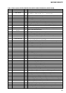
Pin No. Pin Name I/O Description
1PAUSE KEY I Set key input terminal (X key input)
2 (MIC SENSE) O
Control signal output to the microphone amp
“H”: HIGH, “L”: LOW, normally: “H” Not used (open)
3 XTEST I Input terminal for the test mode set up “L”: test mode (normally fixed at “H”)
4, 5 NC O Not used (open)
6 MCUVDD0 — Power supply terminal (for microcomputer block) (+1.5 V)
7 MIFVSS3 — Ground terminal (for microcomputer I/F)
8 XRST I System reset signal input terminal from the power control (IC901) “L”: reset
9S MON I Servo signal monitor input terminal (A/D input) from RF amp (IC501)
10 VB MON I Voltage monitor input terminal of UNREG power supply (A/D input)
11 CHG MON I Charge voltage monitor input terminal (A/D input) Not used (open)
12 VREF MON I Clear reference voltage input terminal (A/D input) from RF amp (IC501)
13, 14
SET KEY 1,
I Set key input terminal (A/D input)
SET KEY 2
15 VL MON I VL voltage monitor input terminal (A/D input)
16 HIDC MON I HIGH DC voltage monitor input terminal (A/D input)
17 WK DET I Set key start switching detection signal input terminal (A/D input)
18 REC KEY I REC key input terminal (A/D input)
19 HALF LOCK SW I
Open button detection switch (S805) input terminal (A/D input)
“L”: when normal position, “H”: when locked
20 RMC KEY I Key input terminal (A/D input) of the remote commander attached headphone
21 AVDD — Power supply terminal (for the analog circuit block) (+2.8 V)
22 AVSS — Ground terminal (for the analog circuit block)
23 VDIOSC — Power supply terminal (for OSC cell) (+2.4 V)
24 OSCI I System clock (45.1584 MHz) input terminal
25 OSCO O System clock (45.1584 MHz) output terminal
26 VSIOSC — Ground terminal (for OSC cell)
27 DAVDD — Power supply terminal (for the built-in D/A converter) (+2.4 V)
28 VREFL I Reference voltage input terminal (for the internal D/A converter L-CH)
29 AOUTL O Built-in D/A converter (L-CH) output terminal
30 AOUTR O Built-in D/A converter (R-CH) output terminal
31 VREFR I Reference voltage input terminal (for the built-in D/A converter R-CH)
32 DAVSS — Ground terminal (for the built-in D/A converter)
33 ASYO O Playback EFM duplex signal output terminal
34 ASYI I Playback EFM comparison slice level input terminal
35 AVD1 — Ground terminal (for the analog) (+2.4 V)
36 BIAS I Bias input for the playback EFM comparison
37 RFI I Playback EFM RF signal input from RF amp (IC501)
38 AVS1 — Ground terminal (for the analog)
39 PCO O Phase comparison output for the master clock of playback EFM system master PLL
40 PDO O Phase comparison output for the analog PLL Not used (open)
41 FILI I Filter input for the master clock of the playback EFM system master PLL
42 FILO O Filter output for the master clock of the playback EFM system master PLL
43 CLTV I Internal VCO control voltage input for the playback EFM system master PLL
44 PEAK I Peak hold signal input of the light amount signal (RF/ABCD) from RF amp (IC501)
45 BOTM I Bottom hold signal input of the light amount signal (RF/ABCD) from RF amp (IC501)
46 ABCD I Light amount signal (ABCD) input from RF amp (IC501)
47 FE I Focus error signal input from RF amp (IC501)
48 AUX1 I Support signal (I3 signal/temperature signal) input terminal (A/D input)
49 VC I Middle point voltage (+1.2 V) input terminal
50 ADIO O Monitor output of A/D converter input signal Not used (open)
51 ADRT I A/D converter the upper limit voltage input (fixed at “H” in this set)