


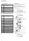
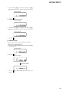

26
MZ-R501/R501PC
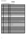
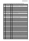
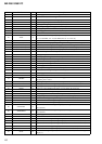
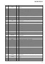
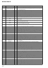
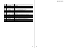
Pin No. Pin Name I/O Description
52 AVD2 — Power supply terminal (for the analog) (+2.4 V)
53 AVS2 — Ground terminal (for the analog)
54 ADRB I A/D converter the lower limit voltage input (fixed at “L” in this set)
55 SE I Sled error signal input terminal Not used (fixed at “L”)
56 TE I Tracking error signal input from RF amp (IC501)
57 DCHG — Connecting analog power supply of the low impedance (fixed at “H” in this set)
58 APC I Error signal input for the laser automatic power control Not used (fixed at “H”)
59 DSPVDD0 — Power supply terminal (for DSP block) (+1.5 V)
60 DSPVSS0 — Ground terminal (for DSP block)
61 XTSL I
Input terminal for the frequency set up of the system clock
“L”: 45.1584 MHz, “H”: 22.5792 MHz (fixed at “L” in this set)
62 DIN1 I Input terminal of the record system digital audio signal
63 (DOUT) O Output terminal of the playback system digital audio signal Not used (open)
64 (DAPWMLP) O D/A converter PWM output (L-CH right phase) Not used (open)
65 (DAPWMLN) O D/A converter PWM output (L-CH reverse phase) Not used (open)
66 (DAPWMRP) O D/A converter PWM output (R-CH right phase) Not used (open)
67 DADT O Audio data output Not used (open)
68 ADDT I Data signal input from the external A/D converter (IC301)
69 LRCK O L/R sampling block signal (44.1 kHz) output to the external A/D converter (IC301)
70 XBCK O Bit clock signal (2.8224 MHz) output to the external A/D converter (IC301)
71 FS256 O 11.2896 MHz clock signal output to the external A/D converter (IC301)
72 (MVCI) I Vibrate input for the digital in PLL from the external VCO Not used (fixed at “L”)
73 DSPVDD1 — Power supply terminal (for DSP block) (+1.5 V)
74 ADFG I ADIP duplex FM signal (20.05 ± 1 kHz) input from RF amp (IC501)
75 (F0CNT) O Filter cut off control signal output Not used (open)
76 DIFVDD0 — Power supply terminal (for DSP I/F) (+2.3 V)
77 DIFVSS0 — Ground terminal (for DSP I/F)
78 APCREF O
Control signal output to the reference voltage generation circuit for the laser
automatic power control
79 (LDDR) O PWM signal output for the laser automatic power control Not used (open)
80 TRDR O Tracking servo drive PWM signal output (–) to the motor driver (IC701)
81 TFDR O Tracking servo drive PWM signal output (+) to the motor driver (IC701)
82 FFDR O Focus servo drive PWM signal output (+) to the motor driver (IC701)
83 FRDR O Focus servo drive PWM signal output (–) to the motor driver (IC701)
84 MCUVDD1 — Power supply terminal (for the microcomputer block) (+1.5 V)
85 (FGIN) I FG signal input terminal for the spindle servo Not used (open)
86 FS4 O 176.4 MHz clock signal output to the power control (IC601, IC901)
87 SPRD/SPDU/RTG0 O Spindle servo drive PWM signal output terminal (–) to the motor driver (IC701)
88 SPFD/SPVS/PWM3 O Spindle servo drive PWM signal output (+)
89 SPDV/RTG1 O
Spindle motor drive control signal output (V)/RTG output 1 to the motor
driver (IC701)
90 SPDW/RTG2 O
Spindle motor drive control signal output (W)/RTG output 2 to the motor
driver (IC701)
91 DSPVDD2 — Power supply terminal (for DSP block) (+1.5 V)
92 DSPVSS1 — Ground terminal (for DSP block)
93 SPCU I Spindle motor drive comparison signal input (U) from the motor driver (IC701)
94 SPCV I Spindle motor drive comparison signal input (V) from the motor driver (IC701)
95 SPCW I Spindle motor drive comparison signal input (W) from the motor driver (IC701)
96 SRDR O Sled servo drive PWM signal output (–) to the motor driver (IC701)
97 SFDR O Sled servo drive PWM signal output (+) to the motor driver (IC701)
98 SLDV O
Sled motor drive signal output (V) to the motor driver (IC701)/drive control signal
output (1–)