


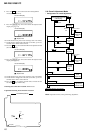

28
MZ-R501/R501PC
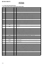
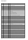
Pin No. Pin Name I/O Description
169 CLK SEL O System clock select signal output to the power control (IC901)
170 OPEN CLOSE SW I
Open/close detection switch (S806) of the upper panel input terminal (A/D input)
“L”: when upper panel close
171 GND SW O Control signal output to the ground (GND) changeover switch
172 SET CODE0 O Input terminal for the set (fixed at “L” in this set)
173, 174 SET CODE1, 2 O Input terminal for the set (open in this set)
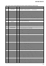
175 SET CODE3 O Input terminal for the set (fixed at “L” in this set)
176 MIFVDD1 — Power supply terminal (for the microcomputer I/F block) (+2.3 V)
177 MIFVSS1 — Ground terminal (for the microcomputer I/F block)
178 (AOUT SEL) O HP/LINE changeover signal output Not used (open)
179 SI0 I
Serial data input from the nonvolatile memory (IC804) and liquid crystal display
element module
180 SO0 O
Serial data output to the nonvolatile memory (IC804), A/D converter (IC301) and
liquid crystal display element module
181 SCK0 O
Serial clock signal output to the nonvolatile memory (IC804), A/D converter (IC301)
and liquid crystal display element module
182 (XGUM ON) I
Battery pack detection switch input terminal for the charge
“L”: there is battery pack for the charge Not used (open)
183 BEEP O Beep sound control signal output Not used (open)
184 NC O Not used (open)
185 VD SEL O VD power supply changeover signal output terminal Not used (open)
186 (XMUTE) O Analog muting control signal output terminal “L”: muting ON Not used (open)
187 LCD RST AUX O Reset control signal output terminal to the liquid crystal display element “L”: reset
188, 189 NC O Not used (open)
190 XPATCH I Patch function detection input terminal “L”: patch function Fixed at “L” in this set
191 OPT DET I DIN plug detection signal input terminal
192 XJACK DET I LINE IN plug detection signal input terminal
193 (XMIC DET) I Microphone plug detection signal input terminal Not used (open)
194, 195 PD S0, PD S1 O PD IC mode changeover signal output to the optical pick up
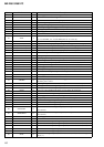
196 MIFVDD2 — Power supply terminal (for the microcomputer I/F block) (+2.3 V)
197 to 199 MODE1 to 3 O
Power supply control signal output (for the over write head drive) to the over write
head drive (IC601)
200, 201 HD CON 1, 2 O Over write head control signal output to the over write head drive (IC601)
202 REC WBL SW O LPF changeover switch input terminal when REC/PB control Not used (open)
203 XCS ADA O Chip select signal output to A/D converter (IC301)
204 XPD ADA O Power supply control signal output for the drive to A/D converter (IC301)
205 XCS LCD O Chip select signal output to the liquid crystal display element
206 LCD STB O Strobe signal output to the the liquid crystal display element
207 LCD RST O Reset control signal output to the liquid crystal display element Not used (open)
208 (REC LED) O LED ON/OFF control signal output for REC display Not used (open)
209 (LD ON) O ON/OFF control signal output terminal of the laser diode Not used (open)
210 (TSB SLV CHK) I TSB slave detection signal input terminal
211, 212 (K-TAI-MON), (K-TAI-SW) I Not used (open)
213 MCUVSS1 — Ground terminal (for the microcomputer block)
214 CAV CLV SW O CAV/CLV changeover control signal output Not used (open)
215 XOPT CTL O Power supply ON/OFF control signal output for DIN PD drive
216 (CS RTC) O Chip select signal output to the clock IC Not used (open)
217 OFTRK I Off track signal input from RF amp (IC501)
218 MUTE O Analog muting control signal output “H”: muting ON
219 XCS NV O Chip select signal output to EEPROM (IC804)
220 XRST MTR DRV O Reset control signal output to the motor driver (IC701)
221 XRF RST O Reset control signal output to RF amp (IC501)
222 MCUVDD3 — Power supply terminal (for the microcomputer block) (+1.5 V)