


1-6 Computer Group Literature Center Web Site
Board Description and Memory Maps
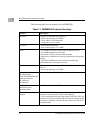
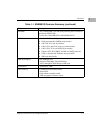
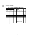
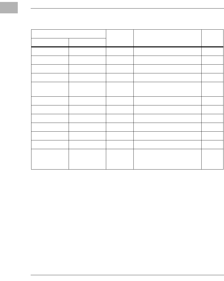
1
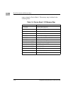
Note Set by configuration resistors.
2800 0000 29FF FFFF 32M PCI Bus 1 Memory Space 3
2A00 0000 41FF FFFF 384M Unassigned
4200 0000 4303 FFFF 256K MV64360 Integrated SRAM
4304 0000 F0FF FFFF 2783M Unassigned
F100 0000 F100 FFFF 64K Internal Registers See
Note
F101 0000 F1FF FFFF 16M-64K Unassigned
F200 0000 F3FF FFFF 32M PCI Bus 0 Memory Space 1
F400 0000 F5FF FFFF 32M PCI Bus 0 Memory Space 2
F600 0000 F7FF FFFF 32M PCI Bus 0 Memory Space 3
F800 0000 FEFF FFFF 112M Unassigned
FF00 0000 FF7F FFFF 8M Device CS3*
FC00 0000 FFFF FFFF 64M Boot Flash (Bank A or B
depending on S4:3 switch
setting)
Table 1-2. Default Processor Address Map (continued)
Processor Address
Size Definition
Notes
Start End