


Time Base Enable Register
http://www.motorola.com/computer/literature 1-19
1
Time Base Enable Register
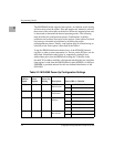
The time base enable (TBEN) register provides the means to control the
processor’s TBEN input.
TBEN0
Processor 0 time base enable. When this bit is cleared, the TBEN pin
of processor 0 is driven low. When this bit is set, the TBEN pin is
driven high.
TBEN1
Not used on the MVME6100.
Quad Universal Asynchronous Receiver/Transmitter (UART)
The MVME6100 board contains one EXAR ST16C554D Quad UART
device connected to the MV64360 device controller bus to provide
asynchronous debug ports. The Quad UART supports up to four
asynchronous serial ports of which two are used on the MVME6100. The
ST16C554D is a universal asynchronous receiver and transmitter and is an
enhanced UART with 16 byte FIFOs, receive trigger levels, and data rates
up to 1.5 Mbps. Onboard status registers provide the user with error
indications, operational status, and modem interface control. System
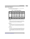
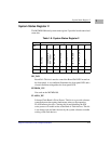
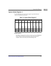
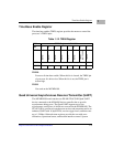
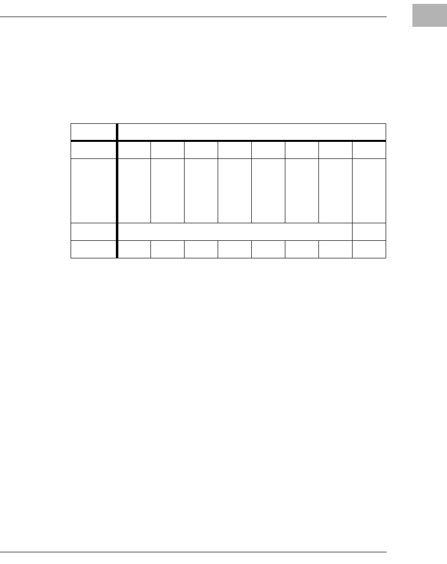
Table 1-12. TBEN Register
REG TBEN Register - 0xF1100006
BIT 76543210
FIELD
RSVD
RSVD
RSVD
RSVD
RSVD
RSVD
TBEN1
(NOT USED)
TBEN0
OPER R/W
RESET 11111XX1