


2-6 Computer Group Literature Center Web Site
Programming Details
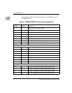
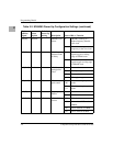
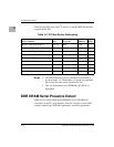
2
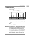
AD[18] Resistor 1 DRAM Clock
Select
0 DRAM is running at a
higher frequency than the
core clock
1 DRAM is running at a same
frequency as the core clock
AD[19] Resistor 1 DRAM
Address/Contr
ol Delay
0 DRAM address and control
signals toggle on falling
edge of DRAM clock
1 DRAM address and control
signals toggle on rising edge
of DRAM clock
AD[21:20] Resistors 01 DRAM control
path pipeline
select
00 Reserved
01 Two Pipe stages
10 Reserved
11 Three pipe stages
AD[24:22] Resistors 000 DRAM read
path control
000
100
DRAM running in sync
mode
001
111
DRAM running in async
mode
AD[25] Fixed 0 Gigabit port 3
Enable
0 Disable
1Enable
AD[28:26] Resistors 101 PCI_1 DLL
control
000 DLL disable
001 Conventional PCI mode at
66MHz
101 PCI-X mode at 133 MHz
110 PCI-X mode at 66 MHz
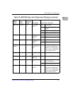
Table 2-2. MV64360 Power-Up Configuration Settings (continued)
Device
AD Bus
Signal
Select
Option
Default
Power-Up
Setting Description State of Bit vs. Function