


1-8 Computer Group Literature Center Web Site
Board Description and Memory Maps
1
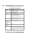
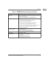
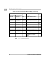
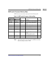
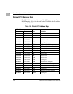
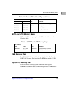
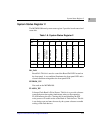
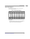
Default PCI Memory Map
The MV64360 presents the following default PCI memory map after
RESET negation. Note: it is the same as the GT-64260A with the addition
of integrated SRAM.
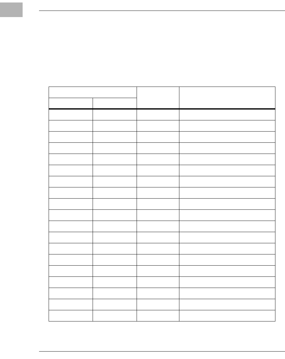
Table 1-4. Default PCI Address Map
PCI Address
Size DefinitionStart End
0000 0000 007F FFFF 8M DRAM Bank 0
0080 0000 00FF FFFF 8M DRAM Bank 1
0100 0000 017F FFFF 8M DRAM Bank 2
0180 0000 01FF FFFF 8M DRAM Bank 3
0200 0000 0FFF FFFF 224M Unassigned
1000 0000 11FF FFFF 32M PCI Bus 1 P2P I/O Space
1200 0000 13FF FFFF 32M PCI Bus 1 P2P Memory Space 0
1400 0000 1400 FFFF 64K Internal Registers
1401 0000 1BFF FFFF 128M-64K Unassigned
1C00 0000 1C7F FFFF 8M Device CS0*
1C80 0000 1CFF FFFF 8M Device CS1*
1D00 0000 1DFF FFFF 16M Device CS2*
1E00 0000 1FFF FFFF 32M Unassigned
2000 0000 21FF FFFF 32M PCI Bus 0 P2P I/O Space
2200 0000 23FF FFFF 32M PCI Bus 0 P2P Memory Space 0
2400 0000 25FF FFFF 32M PCI Bus 0 P2P Memory Space 1
2600 0000 41FF FFFF 448M Unassigned
4200 0000 4303 FFFF 256K MV64360 Integrated SRAM
4304 0000 F1FF FFFF 2800M Unassigned