


2-8 Computer Group Literature Center Web Site
Programming Details
2
Flash Memory
The MVME6100 contains two banks of flash memory accessed via the
Device Controller bus contained within MV64360. Each bank contains
from 8MB to 64MB of 32-bit wide Boot Block flash memory provided by
two 16-bit wide Intel StrataFlash devices.
The Boot Bank is jumper selectable to select either flash bank as the boot
bank. The jumper effectively swaps the chip selects to the two flash banks
so that either bank can be used as the boot bank. The state of the jumper is
readable in the BANK_SELECT bit of System Status Register 1 to
properly set up the MV64360 Device Controller Bus memory maps.
The boot device bank is the same as any of the other device banks except
that its default address map matches the PowerPC CPU boot address
(0xfff0.0100) and that its default width is sampled at reset.
Real-Time Clock and NVRAM
The Real-Time Clock/NVRAM/Watchdog Timer is implemented using a
SGS-Thompson M48T37V Timekeeper SRAM, and M4T28-BR12SH1
SnapHat battery. Refer to the M48T37V data sheets for additional
programming information. Refer to Appendix A, Related Documentation.
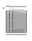
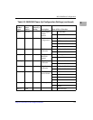
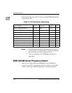
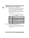
TxD0[7] Resistor 0 JTAG Pad
Calib Bypass
0 Normal Operation
1 Bypass pad calibration
TxD1[1] Resistor 0 Core PLL
Bypass
0 Normal Operation
1 Bypass the core’s PLL
TxD1[4:2] Resistors 000 Core PLL
Control
000 Tuning of the core PLL
clock tree.
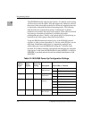
Table 2-2. MV64360 Power-Up Configuration Settings (continued)
Device
AD Bus
Signal
Select
Option
Default
Power-Up
Setting Description State of Bit vs. Function