


Operating Basics
P6330 3.5 GHz Differential Probe Instructi on Manual
11
Maximum Input Voltage
The maximum input voltage is the maximum voltage to ground that
the inputs can withstand without damaging the input circuitry of the
probe.
CAUTION. To avoid damaging the inputs of the P6330 differential
probe, do not apply more than ± 15 V (DC + peak AC) between each
input and ground.
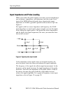
Common-Mode Signal Range
The common-mode signal range is the maximum voltage that you
can apply to each input, wit h respec t to ea rth ground, without
saturating the input circuitry of the probe. A common-mode voltage
that exceeds the common-mode signal range may produce an
erroneous output waveform even when the differential-mode
specification is met. For Specifications, refer to page 25.
Differential-Mode Signal Range
The differential-mode signal range is the maximum voltage
difference between the plus and minus inputs that the probe can
accept without distorting the signal. The distortion from a voltage
that is too large can result in a clipped or otherwise distorted and
inaccurate measurement. For Specifications, refer to page 25.
Common-Mode Rejection
The common-mode rejection ratio (CMRR) is the ability of a probe
to reject signals that are common to both inputs. More precisely,
CMRR is the ratio of the differential gain to the common-mode gain.
The higher the ratio, the greater the ability to reject common-mode
signals.
Common-mode rejection decreases as the input frequency increases.
Figure 11 on page 28 is a plot of typical CMRR of the probe versus
input frequency. For additional information about CMRR, see
page 20.