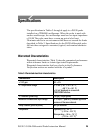
Specifications
P6330 3.5 GHz Differential Probe Instructi on Manual
27
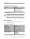
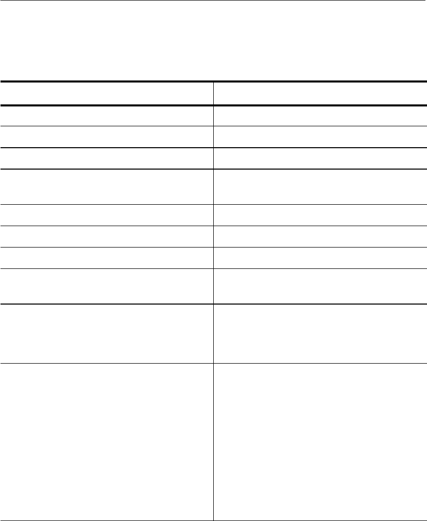
Table 4: Typical electrical characteristics (Cont.)
Characteristic Description
Delay time 5.4 ns
Differential input resistance, DC coupled
100 kΩ ± 2%
Differential input capacitance < 0.3 pF at 100 MHz
Common-mode input resistance, DC
coupled
50 kΩ ± 2% (per side)
Common-mode input capacitance < 0.45 pF at 100 MHz (per side)
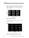
Input impedance SeeFigure12
Noise, referred to input 35 nV/√Hz
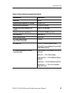
DC Offset Scale Accuracy
(gain of offset signal path)
ᐔ2.0%
DC Offset Drift
150 V/°C or less at output of probe
0.75 mV/°C or less displayed on screen with
TEKPROBE interface
DC Voltage Measurement Accuracy
(referred to input)
ᐔ[2% of input + (2% of offset) + 50.0 mV +
40.0 mV]
gain error = ᐔ2% of input voltage
offset gain error =ᐔ2% of effective offset at
probe tip
output zero = ᐔ50 mV effective at probe tip
linearity error = ᐔ1.0% of 4.0 V dynamic
range (40.0 mV)


