


4−11
4.18 CardBus Latency Timer Register
The CardBus latency timer register is programmed by the host system to specify the latency timer for the
PCI7x21/PCI7x11 CardBus interface, in units of CCLK cycles. When the PCI7x21/PCI7x11 controller is a CardBus
initiator and asserts CFRAME
, the CardBus latency timer begins counting. If the latency timer expires before the
PCI7x21/PCI7x11 transaction has terminated, then the PCI7x21/PCI7x11 controller terminates the transaction at the
end of the next data phase. A recommended minimum value for this register of 20h allows most transactions to be
completed.
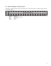
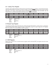
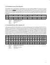
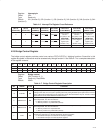
Bit 7 6 5 4 3 2 1 0
Name CardBus latency timer
Type RW RW RW RW RW RW RW RW
Default 0 0 0 0 0 0 0 0
Register: CardBus latency timer
Offset: 1Bh (Functions 0, 1)
Type: Read/Write
Default: 00h
4.19 CardBus Memory Base Registers 0, 1
These registers indicate the lower address of a PCI memory address range. They are used by the PCI7x21/PCI7x11
controller to determine when to forward a memory transaction to the CardBus bus, and likewise, when to forward a
CardBus cycle to PCI. Bits 31−12 of these registers are read/write and allow the memory base to be located anywhere
in the 32-bit PCI memory space on 4-Kbyte boundaries. Bits 11−0 are read-only and always return 0s. Writes to these
bits have no effect. Bits 8 and 9 of the bridge control register (PCI offset 3Eh, see Section 4.25) specify whether
memory windows 0 and 1 are prefetchable or nonprefetchable. The memory base register or the memory limit register
must be nonzero in order for the PCI7x21/PCI7x11 controller to claim any memory transactions through CardBus
memory windows (i.e., these windows by default are not enabled to pass the first 4 Kbytes of memory to CardBus).
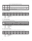
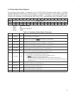
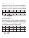
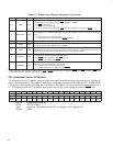
Bit 31 30 29 28 27 26 25 24 23 22 21 20 19 18 17 16
Name Memory base registers 0, 1
Type RW RW RW RW RW RW RW RW RW RW RW RW RW RW RW RW
Default 0 0 0 0 0 0 0 0 0 0 0 0 0 0 0 0
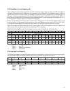
Bit 15 14 13 12 11 10 9 8 7 6 5 4 3 2 1 0
Name Memory base registers 0, 1
Type RW RW RW RW R R R R R R R R R R R R
Default 0 0 0 0 0 0 0 0 0 0 0 0 0 0 0 0
Register: Memory base registers 0, 1
Offset: 1Ch, 24h
Type: Read-only, Read/Write
Default: 0000 0000h