


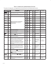
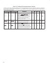


2−26
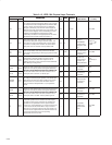
Table 2−15. IEEE 1394 Physical Layer Terminals
TERMINAL
DESCRIPTION
I/O
INPUT
OUTPUT
EXTERNAL
PIN STRAPPING
NAME NO.
DESCRIPTION
I/O
TYPE
INPUT OUTPUT
EXTERNAL
COMPONENTS
PIN STRAPPING
(IF USED)
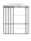
CNA P15
Cable not active. This terminal is asserted high when there
are no ports receiving incoming bias voltage. If it is not used,
then this terminal must be strapped either to DVDD or GND
through a resistor. The CNA terminal can be disabled by
setting bit 7 (CNAOUT) of the PCI PHY control register at
offset ECh in the PCI configuration space (see Section 7.22,
PCI PHY Control Register). This bit is loaded by the serial
EEPROM. If an EEPROM is implemented and CNA
functionality is needed, then the appropriate bit in the serial
EEPROM must be cleared as defined in Table 3−9.
I/O LVCO1 Tie to GND
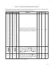
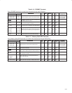
CPS M11
Cable power status input. This terminal is normally
connected to cable power through a 400-kΩ resistor. This
circuit drives an internal comparator that is used to detect
the presence of cable power. If CPS is not used to detect
cable power, then this terminal must be pulled to GND.
FT FT
390-kΩ series
resistor to
BUSPOWER if
providing power
through the 1394
port
Pullup to V
CC
through 1-kΩ
resistor
PC0
PC1
PC2
R12
U13
V13
Power class programming inputs. On hardware reset, these
inputs set the default value of the power class indicated
during self-ID. Programming is done by tying these terminals
high or low.
I LVCI1
Pullup resistors if
high. Can be tied
directly to ground
if set to low.
Tie to GND
R0
R1
U18
U19
Current-setting resistor terminals. These terminals are
connected to an external resistance to set the internal
operating currents and cable driver output currents. A
resistance of 6.34 kΩ ±1% is required to meet the IEEE Std
1394-1995 output voltage limits.
—
6.34-kΩ ±1%
resistor between
R0 and R1 per
1394 specification
Float
Pull directly to
V
CC
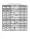
TPA0P
TPA0N
V15
W15
Twisted-pair cable A differential signal terminals. Board trace
lengths from each pair of positive and negative differential
signal pins must be matched and as short as possible to the
I/O
1394 termination
(see reference
schematics)
Float
TPA1P
TPA1N
V18
W18
signal pins must be matched and as short as possible to the
external load resistors and to the cable connector. For an
unused port, TPA+ and TPA− can be left open.
I/O
1394 termination
(see reference
schematics)
Float
TPBIAS0
TPBIAS1
U15
U17
Twisted-pair bias output. This provides the 1.86-V nominal
bias voltage needed for proper operation of the twisted-pair
cable drivers and receivers and for signaling to the remote
nodes that there is an active cable connection. Each of
these pins must be decoupled with a 1.0-µF capacitor to
ground.
I/O
1394 termination
(see reference
schematics)
Float
TPB0P
TPB0N
V14
W14
Twisted-pair cable B differential signal terminals. Board trace
lengths from each pair of positive and negative differential
signal pins must be matched and as short as possible to the
I/O
1394 termination
(see reference
schematics)
Tie to GND
TPB1P
TPB1N
V16
W16
signal pins must be matched and as short as possible to the
external load resistors and to the cable connector. For an
unused port, TPB+ and TPB− must be pulled to ground.
I/O
1394 termination
(see reference
schematics)
Tie to GND
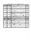
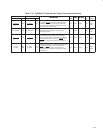
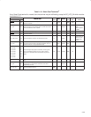
XI
XO
R18
R19
Crystal oscillator inputs. These pins connect to a
24.576-MHz parallel resonant fundamental mode crystal.
The optimum values for the external shunt capacitors are
dependent on the specifications of the crystal used (see
Section 3.9.2, Crystal Selection). An external clock input can
be connected to the XI terminal. When using an external
clock input, the XO terminal must be left unconnected, and
the clock must be supplied before the controller is taken out
of reset. Refer to Section 3.9.2 for the operating
characteristics of the XI terminal.
—
24.576-MHz
oscillator (see
implementation
guide)
Tie to GND
Float