


4−32
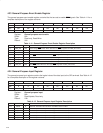
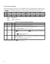
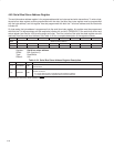
4.43 Power Management Capabilities Register
The power management capabilities register contains information on the capabilities of the PC Card function related
to power management. Both PCI7x21/PCI7x11 CardBus bridge functions support D0, D1, D2, and D3 power states.
Default register value is FE12h for operation in accordance with PCI Bus Power Management Interface Specification
revision 1.1. See Table 4−19 for a complete description of the register contents.
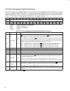
Bit 15 14 13 12 11 10 9 8 7 6 5 4 3 2 1 0
Name Power management capabilities
Type RW R R R R R R R R R R R R R R R
Default 1 1 1 1 1 1 1 0 0 0 0 1 0 0 1 0
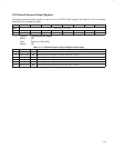
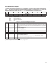
Register: Power management capabilities
Offset: A2h (Functions 0, 1)
Type: Read-only, Read/Write
Default: FE12h
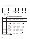
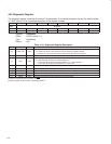
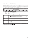
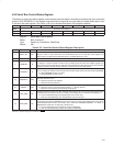
Table 4−19. Power Management Capabilities Register Description
BIT
SIGNAL TYPE FUNCTION
This 5-bit field indicates the power states from which the PCI7x21/PCI7x11 controller functions can assert
PME
. A 0 for any bit indicates that the function cannot assert the PME signal while in that power state.
These 5 bits return 11111b when read. Each of these bits is described below:
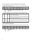
15 ‡
PME support
RW Bit 15 − defaults to a 1 indicating the PME signal can be asserted from the D3
cold
state. This bit is read/write
because wake-up support from D3
cold
is contingent on the system providing an auxiliary power source
to the V
CC
terminals. If the system designer chooses not to provide an auxiliary power source to the V
CC
terminals for D3
cold
wake-up support, then BIOS must write a 0 to this bit.
14−11 R Bit 14 − contains the value 1 to indicate that the PME signal can be asserted from the D3
hot
state.
Bit 13 − contains the value 1 to indicate that the PME
signal can be asserted from the D2 state.
Bit 12 − contains the value 1 to indicate that the PME
signal can be asserted from the D1 state.
Bit 11 − contains the value 1 to indicate that the PME
signal can be asserted from the D0 state.
10 D2_Support R This bit returns a 1 when read, indicating that the function supports the D2 device power state.
9 D1_Support R This bit returns a 1 when read, indicating that the function supports the D1 device power state.
8−6 RSVD R Reserved. These bits return 000b when read.
5 DSI R Device-specific initialization. This bit returns 0 when read.
4 AUX_PWR R
Auxiliary power source. This bit is meaningful only if bit 15 (D3
cold
supporting PME) is set. When this bit
is set, it indicates that support for PME
in D3
cold
requires auxiliary power supplied by the system by way
of a proprietary delivery vehicle.
A 0 (zero) in this bit field indicates that the function supplies its own auxiliary power source.
If the function does not support PME while in the D3
cold
state (bit 15=0), then this field must always return
0.
3 PMECLK R
When this bit is 1, it indicates that the function relies on the presence of the PCI clock for PME operation.
When this bit is 0, it indicates that no PCI clock is required for the function to generate PME
.
Functions that do not support PME generation in any state must return 0 for this field.
2−0 Version R
These 3 bits return 010b when read, indicating that there are 4 bytes of general-purpose power
management (PM) registers as described in draft revision 1.1 of the PCI Bus Power Management Interface
Specification.
‡
This bit is cleared only by the assertion of GRST
.