


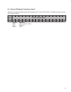
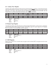

4−6
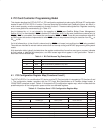
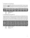
Table 4−4. Status Register Description (continued)
BIT SIGNAL TYPE FUNCTION
4 CAPLIST R
Capabilities list. This bit returns 1 when read. This bit indicates that capabilities in addition to standard PCI
capabilities are implemented. The linked list of PCI power-management capabilities is implemented in this
function.
3 INT_STATUS RU
Interrupt status. This bit reflects the interrupt status of the function. Only when bit 10 (INT_DISABLE) in the
command register (PCI offset 04h, see Section 4.4) is a 0 and this bit is a 1, is the function’s INTx
signal
asserted. Setting the INT_DISABLE bit to a 1 has no effect on the state of this bit.
2−0 RSVD R Reserved. These bits return 0s when read.
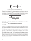
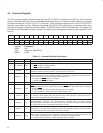
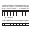
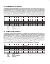
4.6 Revision ID Register
The revision ID register indicates the silicon revision of the PCI7x21/PCI7x11 controller.
Bit 7 6 5 4 3 2 1 0
Name Revision ID
Type R R R R R R R R
Default 0 0 0 0 0 0 0 0
Register: Revision ID
Offset: 08h (functions 0, 1)
Type: Read-only
Default: 00h
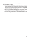
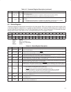
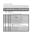
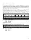
4.7 Class Code Register
The class code register recognizes PCI7x21/PCI7x11 functions 0 and 1 as a bridge device (06h) and a CardBus
bridge device (07h), with a 00h programming interface.
Bit 23 22 21 20 19 18 17 16 15 14 13 12 11 10 9 8 7 6 5 4 3 2 1 0
Name PCI class code
Base class Subclass Programming interface
Type R R R R R R R R R R R R R R R R R R R R R R R R
Default 0 0 0 0 0 1 1 0 0 0 0 0 0 1 1 1 0 0 0 0 0 0 0 0
Register: PCI class code
Offset: 09h (functions 0, 1)
Type: Read-only
Default: 06 0700h
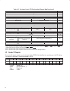
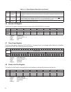
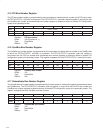
4.8 Cache Line Size Register
The cache line size register is programmed by host software to indicate the system cache line size.
Bit 7 6 5 4 3 2 1 0
Name Cache line size
Type RW RW RW RW RW RW RW RW
Default 0 0 0 0 0 0 0 0
Register: Cache line size
Offset: 0Ch (Functions 0, 1)
Type: Read/Write
Default: 00h