


3−20
The INTRTIE and TIEALL bits affect the read-only value provided through accesses to the interrupt pin register (PCI
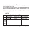
offset 3Dh, see Section 4.24). Table 3−12 summarizes the interrupt signaling modes.
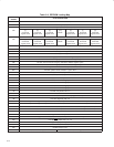
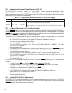
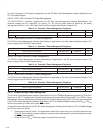
Table 3−12. Interrupt Pin Register Cross Reference
INTRTIE
Bit
TIEALL
Bit
INTPIN
Function 0
(CardBus)
INTPIN
Function 1
(CardBus)
INTPIN
Function 2
(1394 OHCI)
INTPIN
Function 3
(Flash Media)
INTPIN
Function 4
(SD Host)
INTPIN
Function 5
(Smart Card)
0 0 0x01 (INTA) 0x02 (INTB) 0x03 (INTC)
Determined by bits
6−5 (INT_SEL field) in
flash media general
Determined by bits
6−5 (INT_SEL field) in
SD host general
Determined by bits
6−5 (INT_SEL field) in
Smart Card general
1 0 0x01 (INTA) 0x01 (INTA) 0x03 (INTC)
flash media general
control register (see
Section 11.21)
SD host general
control register (see
Section 12.22)
Smart Card general
control register (see
Section 13.22)
X 1 0x01 (INTA) 0x01 (INTA) 0x01 (INTA) 0x01 (INTA) 0x01 (INTA) 0x01 (INTA)
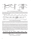
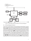
3.7.5 Using Serialized IRQSER Interrupts
The serialized interrupt protocol implemented in the PCI7x21/PCI7x11 controller uses a single terminal to
communicate all interrupt status information to the host controller. The protocol defines a serial packet consisting of
a start cycle, multiple interrupt indication cycles, and a stop cycle. All data in the packet is synchronous with the PCI
clock. The packet data describes 16 parallel ISA IRQ signals and the optional 4 PCI interrupts INTA
, INTB, INTC, and
INTD
. For details on the IRQSER protocol, refer to the document Serialized IRQ Support for PCI Systems.
3.7.6 SMI Support in the PCI7x21/PCI7x11 Controller
The PCI7x21/PCI7x11 controller provides a mechanism for interrupting the system when power changes have been
made to the PC Card socket interfaces. The interrupt mechanism is designed to fit into a system maintenance
interrupt (SMI) scheme. SMI interrupts are generated by the PCI7x21/PCI7x11 controller, when enabled, after a write
cycle to either the socket control register (CB offset 10h, see Section 6.5) of the CardBus register set, or the ExCA
power control register (ExCA offset 02h/42h/802h, see Section 5.3) causes a power cycle change sequence to be
sent on the power switch interface.
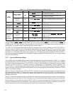
The SMI control is programmed through three bits in the system control register (PCI offset 80h, see Section 4.29).
These bits are SMIROUTE (bit 26), SMISTATUS (bit 25), and SMIENB (bit 24). Table 3−13 describes the SMI control
bits function.
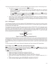
Table 3−13. SMI Control
BIT NAME FUNCTION
SMIROUTE This shared bit controls whether the SMI interrupts are sent as a CSC interrupt or as IRQ2.
SMISTAT This socket-dependent bit is set when an SMI interrupt is pending. This status flag is cleared by writing back a 1.
SMIENB When set, SMI interrupt generation is enabled. This bit is shared by functions 0 and 1.
If CSC SMI interrupts are selected, then the SMI interrupt is sent as the CSC on a per-socket basis. The CSC interrupt
can be either level or edge mode, depending upon the CSCMODE bit in the ExCA global control register (ExCA offset
1Eh/5Eh/81Eh, see Section 5.20).
If IRQ2 is selected by SMIROUTE, then the IRQSER signaling protocol supports SMI signaling in the IRQ2 IRQ/Data
slot. In a parallel ISA IRQ system, the support for an active low IRQ2 is provided only if IRQ2 is routed to either
MFUNC3 or MFUNC6 through the multifunction routing status register (PCI offset 8Ch, see Section 4.36).
3.8 Power Management Overview
In addition to the low-power CMOS technology process used for the PCI7x21/PCI7x11 controller, various features
are designed into the controller to allow implementation of popular power-saving techniques. These features and
techniques are as follows:
• Clock run protocol
• Cardbus PC Card power management
• 16-bit PC Card power management
• Suspend mode