


3−1
3 Feature/Protocol Descriptions
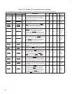
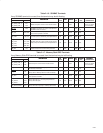
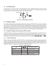
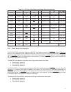
The following sections give an overview of the PCI7x21/PCI7x11 controller. Figure 3−1 shows the connections to the
PCI7x21/PCI7x11 controller. The PCI interface includes all address/data and control signals for PCI protocol. The
interrupt interface includes terminals for parallel PCI, parallel ISA, and serialized PCI and ISA signaling.
PCI Bus
PCI7x21/
PCI7x11
1394a
Socket
EEPROM
Power Switch
SD/MMC
PC
Card/
UltraMedia
Card
Power
Switch
PC
Card/
UltraMedia
Card
Power Switch
SD/MMC
MS/MSPRO
SM/xD
Figure 3−1. PCI7x21/PCI7x11 System Block Diagram
3.1 Power Supply Sequencing
The PCI7x21/PCI7x11 controller contains 3.3-V I/O buffers with 5-V tolerance requiring a core power supply and
clamp voltages. The core power supply is always 1.5 V. The clamp voltages can be either 3.3 V or 5 V, depending
on the interface. The following power-up and power-down sequences are recommended.
The power-up sequence is:
1. Power core 1.5 V.
2. Apply the I/O voltage.
3. Apply the analog voltage.
4. Apply the clamp voltage.
The power-down sequence is:
1. Remove the clamp voltage.
2. Remove the analog voltage.
3. Remove the I/O voltage.
4. Remove power from the core.
NOTE: If the voltage regulator is enabled, then steps 2, 3, and 4 of the power-up sequence
and steps 1, 2, and 3 of the power-down sequence all occur simultaneously.