


12−14
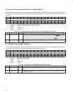
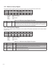
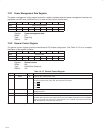
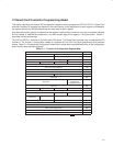
12.21 Power Management Data Register
The power management bridge support extension register provides extended power-management features not
applicable to the SD host controller; thus, it is read-only and returns 0 when read.
Bit 7 6 5 4 3 2 1 0
Name Power management data
Type R R R R R R R R
Default 0 0 0 0 0 0 0 0
Register: Power management data
Offset: 87h
Type: Read-only
Default: 00h
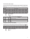
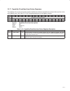
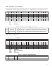
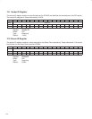
12.22 General Control Register
The general control register provides miscellaneous PCI-related configuration. See Table 12−15 for a complete
description of the register contents.
Bit 7 6 5 4 3 2 1 0
Name General control
Type R RW RW RW RW RW RW RW
Default 0 0 0 0 0 0 0 0
Register: General control
Offset: 88h
Type: Read/Write, Read-only
Default: 00h
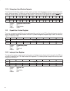
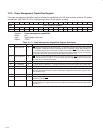
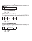
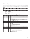
Table 12−15. General Control Register
BIT FIELD NAME TYPE DESCRIPTION
7 RSVD R Reserved. Bit 7 returns 0 when read.
6−5 ‡ INT_SEL RW Interrupt select. These bits are program the INTPIN register and set which interrupt output is used.
This field is ignored if one of the USE_INTx terminals is asserted.
00 = INTA
01 = INTB
10 = INTC
11 = INTD
4 ‡ D3_COLD RW D3
cold
PME support. This bit sets and clears the D3
cold
PME support bit in the power management
capabilities register.
3−1 RSVD R Reserved. Bits 3−1 return 0s when read.
0 ‡ DMA_EN RW DMA enable. This bit enables DMA functionality of the SD host controller core. When this bit is set,
the PGMIF field in the class code register returns 01h and the DMA_SUPPORT bit in the capabilities
register of each SD host socket is set. When this bit is 0, the PGMIF field returns 00h and the
DMA_SUPPORT bit of each SD host socket is 0.
‡
One or more bits in this register are cleared only by the assertion of GRST
.