


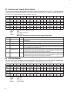
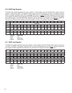

8−14
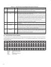
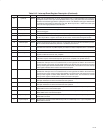
Table 8−11. Host Controller Control Register Description (Continued)
BIT FIELD NAME TYPE DESCRIPTION
22 aPhyEnhanceEnable RSC When bits 23 (programPhyEnable) and 17 (linkEnable) are 1, the OHCI driver can set bit 22 to
1 to use all IEEE 1394a-2000 enhancements. When bit 23 (programPhyEnable) is cleared to 0,
the software does not change PHY enhancements or this bit.
21−20 RSVD R Reserved. Bits 21 and 20 return 0s when read.
19 LPS RSC Bit 19 controls the link power status. Software must set this bit to 1 to permit the link-PHY
communication. A 0 prevents link-PHY communication.
The OHCI-link is divided into two clock domains (PCLK and PHY_SCLK). If software tries to
access any register in the PHY_SCLK domain while the PHY_SCLK is disabled, then a target
abort is issued by the link. This problem can be avoided by setting bit 4 (DIS_TGT_ABT) to 1 in
the PCI miscellaneous configuration register at offset F0h in the PCI configuration space (see
Section 7.23). This allows the link to respond to these types of request by returning all Fs (hex).
OHCI registers at offsets DCh−F0h and 100h−11Ch are in the PHY_SCLK domain.
After setting LPS, software must wait approximately 10 ms before attempting to access any of
the OHCI registers. This gives the PHY_SCLK time to stabilize.
18 postedWriteEnable RSC Bit 18 enables (1) or disables (0) posted writes. Software changes this bit only when bit 17
(linkEnable) is 0.
17 linkEnable RSC Bit 17 is cleared to 0 by either a system (hardware) or software reset. Software must set this bit
to 1 when the system is ready to begin operation and then force a bus reset. This bit is necessary
to keep other nodes from sending transactions before the local system is ready. When this bit is
cleared, the PCI7x21/PCI7x11 controller is logically and immediately disconnected from the 1394
bus, no packets are received or processed, nor are packets transmitted.
16 SoftReset RSCU When bit 16 is set to 1, all PCI7x21/PCI7x11 states are reset, all FIFOs are flushed, and all OHCI
registers are set to their system (hardware) reset values, unless otherwise specified. PCI
registers are not affected by this bit. This bit remains set to 1 while the software reset is in progress
and reverts back to 0 when the reset has completed.
15−0 RSVD R Reserved. Bits 15−0 return 0s when read.
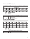
8.17 Self-ID Buffer Pointer Register
The self-ID buffer pointer register points to the 2K-byte aligned base address of the buffer in host memory where the
self-ID packets are stored during bus initialization. Bits 31−11 are read/write accessible. Bits 10−0 are reserved, and
return 0s when read.
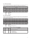
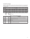
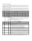
Bit 31 30 29 28 27 26 25 24 23 22 21 20 19 18 17 16
Name Self-ID buffer pointer
Type RW RW RW RW RW RW RW RW RW RW RW RW RW RW RW RW
Default X X X X X X X X X X X X X X X X
Bit 15 14 13 12 11 10 9 8 7 6 5 4 3 2 1 0
Name Self-ID buffer pointer
Type RW RW RW RW RW R R R R R R R R R R R
Default X X X X X 0 0 0 0 0 0 0 0 0 0 0
Register: Self-ID buffer pointer
Offset: 64h
Type: Read/Write, Read-only
Default: XXXX XX00h