


7−11
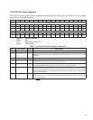
7.16 Minimum Grant and Maximum Latency Register
The minimum grant and maximum latency register communicates to the system the desired setting of bits 15−8 in
the latency timer and class cache line size register at offset 0Ch in the PCI configuration space (see Section 7.6).
If a serial EEPROM is detected, then the contents of this register are loaded through the serial EEPROM interface
after a GRST
. If no serial EEPROM is detected, then this register returns a default value that corresponds to the
MAX_LAT = 4, MIN_GNT = 2. See Table 7−13 for a complete description of the register contents.
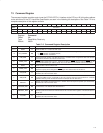
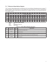
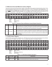
Bit 15 14 13 12 11 10 9 8 7 6 5 4 3 2 1 0
Name Minimum grant and maximum latency
Type RU RU RU RU RU RU RU RU RU RU RU RU RU RU RU RU
Default 0 0 0 0 0 1 0 0 0 0 0 0 0 0 1 0
Register: Minimum grant and maximum latency
Offset: 3Eh
Type: Read/Update
Default: 0402h
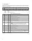
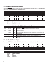
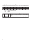
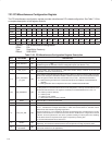
Table 7−13. Minimum Grant and Maximum Latency Register Description
BIT FIELD NAME TYPE DESCRIPTION
15−8 ‡ MAX_LAT RU
Maximum latency. The contents of this field may be used by host BIOS to assign an arbitration priority level
to the PCI7x21/PCI7x11 controller. The default for this register indicates that the PCI7x21/PCI7x11
controller may need to access the PCI bus as often as every 0.25 µs; thus, an extremely high priority level
is requested. Bits 11−8 of this field may also be loaded through the serial EEPROM.
7−0 ‡ MIN_GNT RU
Minimum grant. The contents of this field may be used by host BIOS to assign a latency timer register value
to the PCI7x21/PCI7x11 controller. The default for this register indicates that the PCI7x21/PCI7x11
controller may need to sustain burst transfers for nearly 64 µs and thus request a large value be
programmed in bits 15−8 of the PCI7x21/PCI7x11 latency timer and class cache line size register at offset
0Ch in the PCI configuration space (see Section 7.6). Bits 3−0 of this field may also be loaded through the
serial EEPROM.
‡
These bits are cleared only by the assertion of GRST
.
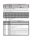
7.17 OHCI Control Register
The PCI OHCI control register is defined by the 1394 Open Host Controller Interface Specification and provides a
bit for big endian PCI support. See Table 7−14 for a complete description of the register contents.
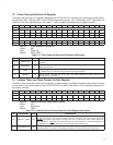
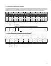
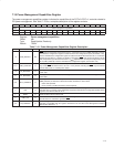
Bit 31 30 29 28 27 26 25 24 23 22 21 20 19 18 17 16
Name OHCI control
Type R R R R R R R R R R R R R R R R
Default 0 0 0 0 0 0 0 0 0 0 0 0 0 0 0 0
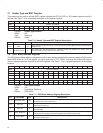
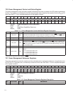
Bit 15 14 13 12 11 10 9 8 7 6 5 4 3 2 1 0
Name OHCI control
Type R R R R R R R R R R R R R R R RW
Default 0 0 0 0 0 0 0 0 0 0 0 0 0 0 0 0
Register: OHCI control
Offset: 40h
Type: Read/Write, Read-only
Default: 0000 0000h
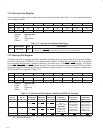
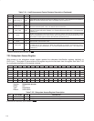
Table 7−14. OHCI Control Register Description
BIT FIELD NAME TYPE DESCRIPTION
31−1 RSVD R Reserved. Bits 31−1 return 0s when read.
0 GLOBAL_SWAP RW
When bit 0 is set to 1, all quadlets read from and written to the PCI interface are byte-swapped (big
endian). The default value for this bit is 0 which is little endian mode.