


2−16
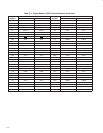
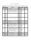
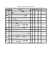
Table 2−7. PCI Address and Data Terminals
Internal pullup/pulldown resistors and pin strapping are not applicable for the PCI address and data terminals.
TERMINAL
DESCRIPTION
I/O
INPUT
OUTPUT
POWER
NAME NO.
DESCRIPTION
I/O
TYPE
INPUT OUTPUT
POWER
RAIL
AD31
AD30
AD29
AD28
AD27
AD26
AD25
AD24
AD23
AD22
AD21
AD20
AD19
AD18
AD17
AD16
AD15
AD14
AD13
AD12
AD11
AD10
AD9
AD8
AD7
AD6
AD5
AD4
AD3
AD2
AD1
AD0
U02
V01
V02
U03
W02
V03
U04
V04
V05
U05
R06
P06
W06
V06
U06
R07
V09
U09
R09
N09
V10
U10
R10
N10
V11
U11
R11
W12
V12
U12
N11
W13
PCI address/data bus. These signals make up the multiplexed PCI address and data bus on the
primary interface. During the address phase of a primary-bus PCI cycle, AD31−AD0 contain a
32-bit address or other destination information. During the data phase, AD31−AD0 contain data.
I/O PCII3 PCIO3 V
CCP
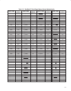
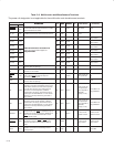
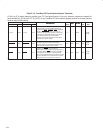
C/BE3
C/BE2
C/BE1
C/BE0
W04
W07
W09
W11
PCI-bus commands and byte enables. These signals are multiplexed on the same PCI
terminals. During the address phase of a primary-bus PCI cycle, C/BE3
−C/BE0 define the bus
command. During the data phase, this 4-bit bus is used as byte enables. The byte enables
determine which byte paths of the full 32-bit data bus carry meaningful data. C/BE0
applies to
byte 0 (AD7−AD0), C/BE1
applies to byte 1 (AD15−AD8), C/BE2 applies to byte 2
(AD23−AD16), and C/BE3
applies to byte 3 (AD31−AD24).
I/O PCII3 PCIO3 V
CCP
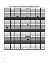
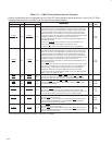
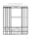
PAR P09
PCI-bus parity. In all PCI-bus read and write cycles, the controller calculates even parity across
the AD31−AD0 and C/BE3
−C/BE0 buses. As an initiator during PCI cycles, the controller
outputs this parity indicator with a one-PCLK delay. As a target during PCI cycles, the controller
compares its calculated parity to the parity indicator of the initiator. A compare error results in
the assertion of a parity error (PERR
).
I/O PCII3 PCIO3 V
CCP