


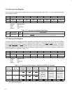
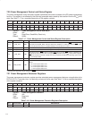
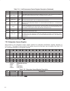
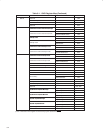

7−18
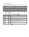
Table 7−21. Link Enhancement Control Register Description (Continued)
BIT FIELD NAME TYPE DESCRIPTION
11 RSVD R Reserved. Bit 11 returns 0 when read.
10 ‡ enab_mpeg_ts RW
Enable MPEG CIP timestamp enhancement. When bit 9 is set to 1, the enhancement is enabled for
MPEG CIP transmit streams (FMT = 20h). The default value for this bit is 0.
9 RSVD R Reserved. Bit 9 returns 0 when read.
8 ‡ enab_dv_ts RW
Enable DV CIP timestamp enhancement. When bit 8 is set to 1, the enhancement is enabled for DV
CIP transmit streams (FMT = 00h). The default value for this bit is 0.
7 ‡ enab_unfair RW
Enable asynchronous priority requests. OHCI-Lynx compatible. Setting bit 7 to 1 enables the link to
respond to requests with priority arbitration. It is recommended that this bit be set to 1. The default value
for this bit is 0.
6 RSVD R
This bit is not assigned in the PCI7x21/PCI7x11 follow-on products, because this bit location loaded
by the serial EEPROM from the enhancements field corresponds to bit 23 (programPhyEnable) in the
host controller control register at OHCI offset 50h/54h (see Section 8.16).
5−3 RSVD R Reserved. Bits 5−3 return 0s when read.
2 ‡ RSVD R Reserved. Bit 2 returns 0 when read.
1 ‡ enab_accel RW
Enable acceleration enhancements. OHCI-Lynx compatible. When bit 1 is set to 1, the PHY layer
is notified that the link supports the IEEE Std 1394a-2000 acceleration enhancements, that is,
ack-accelerated, fly-by concatenation, etc. It is recommended that this bit be set to 1. The default value
for this bit is 0.
0 RSVD R Reserved. Bit 0 returns 0 when read.
‡
This bit is cleared only by the assertion of GRST
.
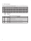
7.25 Subsystem Access Register
Write access to the subsystem access register updates the subsystem identification registers identically to
OHCI-Lynx. The system ID value written to this register may also be read back from this register. See Table 7−22
for a complete description of the register contents.
Bit 31 30 29 28 27 26 25 24 23 22 21 20 19 18 17 16
Name Subsystem access
Type RW RW RW RW RW RW RW RW RW RW RW RW RW RW RW RW
Default 0 0 0 0 0 0 0 0 0 0 0 0 0 0 0 0
Bit 15 14 13 12 11 10 9 8 7 6 5 4 3 2 1 0
Name Subsystem access
Type RW RW RW RW RW RW RW RW RW RW RW RW RW RW RW RW
Default 0 0 0 0 0 0 0 0 0 0 0 0 0 0 0 0
Register: Subsystem access
Offset: F8h
Type: Read/Write
Default: 0000 0000h
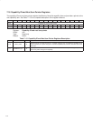
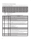
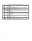
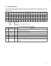
Table 7−22. Subsystem Access Register Description
BIT FIELD NAME TYPE DESCRIPTION
31−16 ‡ SUBDEV_ID RW Subsystem device ID alias. This field indicates the subsystem device ID.
15−0 ‡ SUBVEN_ID RW Subsystem vendor ID alias. This field indicates the subsystem vendor ID.
‡
These bits are cleared only by the assertion of GRST
.